

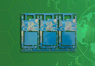

Model : Micro SD card PCB
материал: isola fr408
Layer :6Layers 2+N+2 HDI
цвет: черный / белый
Finished Thickness : 0.3mm
толщина меди: 1 / 3 унции внутри, 0 унций снаружи. унция
обработка поверхности: выщелачивание золота
минимальный трек / пространство: 2.5mil / 2.5mil
Min Hole :Mechanical hole 0.2mm,Laser Hole 0.1mm
Приложение: Micro SDKA PCB
Micro SDCA is a very small flash drive. Its format originated from SanDisk. Initially, it was called T - lightning, and then - trans - lightning. The reason why it was renamed micro SD was adopted by the SD Association (SDA). Other storage cards used in OSD include mini cards and SDKA.
"Micro SD" is mainly used for mobile phones, however due to its small size and high storage capacity it is used for GPS, portable music players and some floppy drives. its volume is 15mm x 11mm x1mm, almost the size of nails. This is currently the minimum storage card.
Micro SD can also be connected to the SD card slot via an SD adapter. MicroSD cards currently have 128MB, 256MB, 512MB, 1g, 2G, 4G, 8g, 16g, 32g, 64g, and 128G capacities (during Mobile World Congress 2014, Sandisk broke with the tradition of storing cards with a maximum capacity of 64 GB and officially released the 128GB micro SD XC memory card.

Micro SD card
SD card pcb design considerations:
1. Attention: the accuracy of the numbering and numbering of paragraphs pcb name. paragraph numbering pcb name include the name of the schematic diagram, schmetic, and the document description part in the lower right corner of the schematic diagram. socket not connected to the network. If there is a network lead connector before, Delete the network name after, there is still a network name, for example. At this point, the Democratic Republic of the Congo made a mistake, and need to delete the lead completely and cross.
2. The documents to be exported for PCB
изготовление, включая файлы Gerber и панельные чертежи. Pay attention to the material requirements to be indicated in the request for opening,the appropriate documents must be installed to configure the card. coordinates must be set to ensure the accuracy of the files. Please note that the main control lamps and lightning bolts should not be close to the edge, but should be reserved at least 0.5 mm of space for production.
4. Export CAD files to the engineering manager with the suffix DXF, Attention, mm.
First, the primary and secondary connections between each signal line should be clearly defined. the main signal line is CLK and VSD. Generally, the Clack signal line should be surrounded by a ground line or ground.
6. After completing all the wiring of ground signal, laying copper wires and observing, so that the ground is as large as possible, the ground between the signal lines is as small as possible, expand the ground area. The ground of the top floor and the bottom floor should be reliably connected. if there is copper on both sides, more holes should be drilled for connection.
As for the breakpoints, they should be as balanced as possible so that they are more sustainable.
Model : Micro SD card PCB
материал: isola fr408
Layer :6Layers 2+N+2 HDI
цвет: черный / белый
Finished Thickness : 0.3mm
толщина меди: 1 / 3 унции внутри, 0 унций снаружи. унция
обработка поверхности: выщелачивание золота
минимальный трек / пространство: 2.5mil / 2.5mil
Min Hole :Mechanical hole 0.2mm,Laser Hole 0.1mm
Приложение: Micro SDKA PCB
For PCB technical problems, iPCB knowledgeable support team is here to help you with every step. You can also request PCB quotation here. Please contact E-mail sales@ipcb.com
We will respond very quickly.


