Digital components are developed as high speed, low power consumption, small size, and high anti-interference ect. The development has influence to the printed circuit baords. There are some suggestions for high-frequency wiring.
(1) High frequency circuit usually with a high degree of integration and wiring density.As wiring is a necessary way to reduce interference,It is necessary to use a multilayer board.
(2) The less circuit bends between the pins(high-speed circuit component ), the better. High frequency circuit wiring are best to be suitable and use full straight lines. But 45-fold lines or arcs can be used. Follow these rules the external emission of high-frequency signals and the coupling between them can be reduced.
(3) The shorter the circuit line between the High frequency circuit board components, the better.
(4) It is better that the circuit of the pins (High frequency circuit components) between layers with less alternation. The “less alternating between layers of leads as possible” means that the fewer vias used in the component deployment process, the better. According to measurements, one via can bring about 0.5 pF of scattered capacitance and reduce damage. The number of vias can increase significantly.
(5) High frequency circuit board wiring should pay attention to the "staggered interference" introduced by signal lines running at a short distance. If there is no way to prevent parallel dispersion, a large plane or the size of the surface of the object can be placed on the opposite side of the parallel signal line Significantly reduce interference. There is almost no way to prevent a flat line in the same layer, but in two adjacent layers, the direction of the line must be vertical to each other.

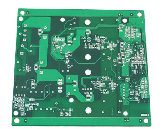
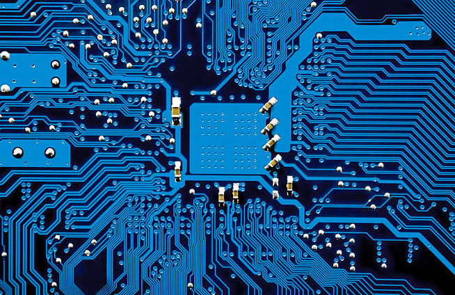
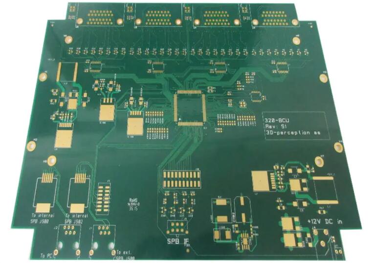
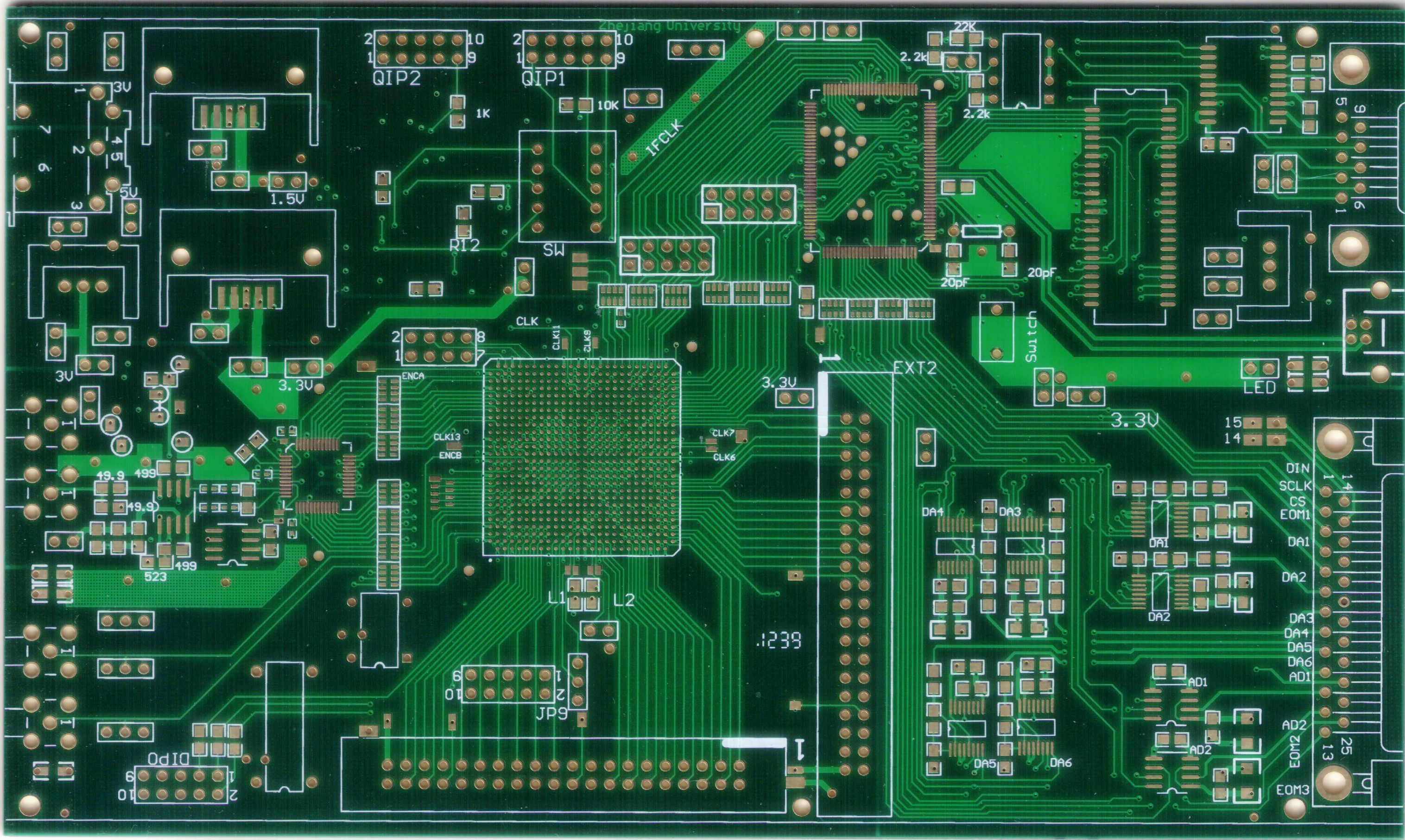
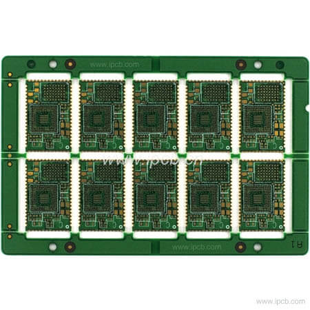
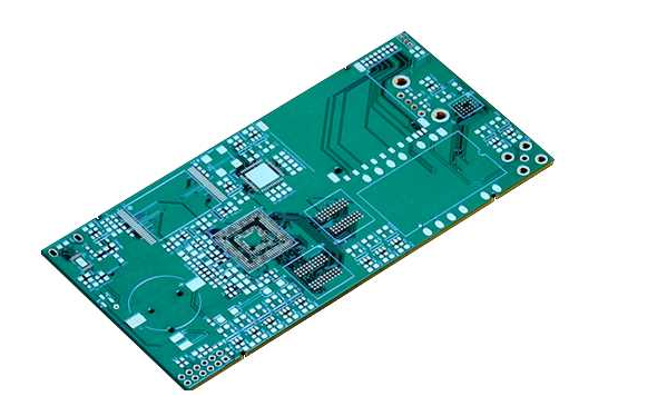
High frequency circuit board
(6) The ground wire envelopment method is applied to signal lines or some units that are particularly tight, that is, to draw the approximate outline of the selected object. Using this function, it can semi-automatically perform the so-called "land-covering" treatment on the selected close signal line. Of course, using this function for time-keeping clocks and other units to perform land-covering treatment will also be very useful for high-speed systems. benefit.
(7) Various types of signal traces cannot form a loop, and the ground cannot form a current loop.
(8) A high-frequency decoupling capacitor should be set near each integrated circuit block.
(9) The High frequency circuit board choke link should be used when the analog ground wire and digital ground wire are connected to the public ground wire. In the actual assembly of high-frequency choke links, high-frequency ferrite gas magnetic beads with core wires perforated are often used. They are generally not represented on the circuit schematic diagram, and the resulting netlist is not used. It contains such components, and it will be ignored due to this when wiring. In view of this fact, it can be regarded as an inductor in the schematic diagram, and a component package is separately defined for it in the PCB component library, and it is manually moved to a suitable location close to the common ground bus junction before wiring.
(10) The simulated circuit and the digital circuit should be placed separately. After independent wiring, the power and ground should be connected at a single point to prevent mutual interference.
(11) Before the DSP, off-chip procedure memory and value memory are connected to the power supply, filter capacitors should be added and they should be made as close as possible to the chip power pins to filter out power supply noise. In addition, shielding is proposed around key parts such as the DSP and off-chip procedure memory and value memory, which can reduce external interference.
(12) The off-chip procedure memory and value memory should be placed as close to the DSP chip as possible, and at the same time, the layout should be reasonable so that the difference between the value line and the address line is basically the same, especially when there are multiple memories in the system. The clock input distance from the clock line to the time of each storage is equivalent or a separate programmable clock drive chip can be added. For a DSP system, an external memory with a similar access speed to the DSP should be selected, otherwise the DSP's high-speed processing experience will not be able to fully perform. The DSP instruction cycle is nanoseconds, so the most obvious problem in DSP hardware systems is high-frequency interference, because when manufacturing printed circuit boards (PCBs) for DSP hardware systems, you should pay attention to address lines and value lines Tighten the wiring of signal lines to be accurate and reasonable. Try to keep the high-frequency lines short and thick when wiring, and keep them away from easily susceptible signal lines, such as analog signal lines. When the surrounding circuits of the DSP are more complicated, it is proposed to make the DSP and its timepiece clock circuit, reset circuit, off-chip procedure memory, and value memory into a minimum system to reduce interference.
(13) In accordance with the above principles, using the technically sophisticated preset tools in the future, and after completing the manual wiring, High frequency circuit board generally need to use advanced PCB simulation in order to increase the reliability and productivity of the system. The software performs simulation.
Due to the limitation of the length of this article, I will give a detailed description of the error and specific simulation, but the proposal for everyone is that if conditions are necessary, the system must be simulated. Here are some basic concepts. Give everyone a basic explanation.