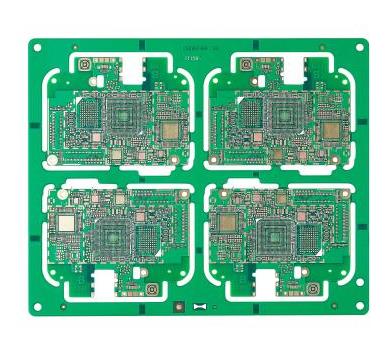
PCB production process flow is different and changing with the progress and difference of PCB type (type) and process technology. At the same time, it is different as PCB manufacturers adopt different process technologies. Different production processes and technology can be used to produce the same or similar PCB products. The traditional production process of single, double, and multilayer boards is still the basis of the PCB production process.

1. Print circuit board. Print out the drawn circuit board with transfer paper, pay attention to the slippery side facing you, generally print two circuit boards, that is, print two circuit boards on one sheet. Choose the circuit board with the best printing effect among them.
2. Cut the copper clad laminate and use the photosensitive board to make the whole process diagram of the circuit board. Copper clad laminate, that is, a circuit board covered with copper films on both sides, cut the copper clad laminate to the size of the circuit board, not too large to save materials.
3. Pretreatment of copper clad laminate. Use fine sandpaper to polish away the oxide layer on the surface of the copper clad laminate to ensure that the carbon powder on the thermal transfer paper can be firmly printed on the copper clad laminate when transferring the circuit board. The standard for polishing is that the board surface is bright without obvious Stains.
4. Transfer circuit board. Cut the printed circuit board to a suitable size, and paste the printed circuit board on the copper clad laminate. After alignment, put the copper clad laminate into the heat transfer machine. Make sure that the transfer paper is not misaligned. Generally, after 2-3 transfers, the circuit board can be transferred firmly on the copper clad laminate. The heat transfer machine has been preheated in advance, and the temperature is set at 160-200 degrees Celsius. Due to the high temperature, pay attention to safety during operation!

5. Corrosion circuit board, reflow soldering machine. First check whether the printed circuit board is completely transferred. If there are a few areas that have not been transferred, use a black oil-based pen to repair. Then it can be corroded. When the exposed copper film on the circuit board is completely corroded, the circuit board is removed from the corrosive solution and cleaned, so that a circuit board is corroded. The composition of the corrosive solution is concentrated hydrochloric acid, concentrated hydrogen peroxide, and water in a ratio of 1:2:3. When preparing the corrosive solution, discharge water first, and then add concentrated hydrochloric acid and concentrated hydrogen peroxide. If the concentrated hydrochloric acid, concentrated hydrogen peroxide or corrosive solution is not Be careful of splashing on the skin or clothing, and wash it with clean water in time. As a strong corrosive solution is used, pay attention to safety during operation!
6. Circuit board drilling. The circuit board needs to be inserted with electronic components, so it is necessary to drill the circuit board. Choose different drill bits according to the thickness of the electronic component pins. When using the drill to drill, the circuit board must be pressed firmly. The drill speed cannot be too slow. Please carefully watch the operator's operation.
7. Circuit board pretreatment. After drilling, use fine sandpaper to polish off the toner on the circuit board, and clean the circuit board with water. After the water dries, apply rosin to the side with the circuit. In order to accelerate the solidification of the rosin, we use a hot air blower to heat the circuit board, and the rosin can solidify in 2-3 minutes. 8. Welding electronic components. After soldering the electronic components on the board, power on. PCB single-sided production process
a. Cut the copper clad laminate; (cut the copper clad board, pay attention to the cutting specifications, and bake the board before cutting);
b. Grinding the plate; (clean the cut copper clad laminate in the plate grinding machine so that the surface is free of dust, burrs and other sundries. The two processes are integrated);
c. Printed circuit; (print the circuit diagram on the side with copper skin, the ink has anti-corrosion effect)
d. Inspection; (remove the excess ink, add ink to the place where the ink is not printed, if a large number of defects are found, adjustments are needed, and the defective products can be placed in the second step of etching for ink cleaning, and can be returned to this channel after cleaning Process reprocessing)
e. The ink is ready to dry;
f. Etching; (use the reagent to corrode the excess copper skin, and the copper skin on the circuit with the ink can be retained, and then use the reagent to clean the ink on the circuit and then dry, these three processes are integrated)
g. Drill positioning holes; (drill positioning holes on the etched board)
h. Grind the board; (clean and dry the board with the positioning hole drilled, the same as the 2 board)
i. Silk screen; (print plug-in component silk screen on the back of the substrate, some marking codes, drying after screen printing, the two processes are integrated)
j. Grinding plate; (clean again)
k. Solder resist; (screen printing green oil solder resist on the cleaned substrate, no green oil is needed at the pads, dry directly after printing, the two processes are integrated)
l. Forming; (Use a punch to form. If there is no need for V-pit treatment, it may be formed in two times. For example, small round plates, first punch from the screen printing surface to the solder mask surface into small circular plates, and then punch from the solder mask surface to the screen printing surface Plug-in hole, etc.)
m. V-pit; (small circular plates do not need V-pit processing, use the machine to cut the substrate out of the board slot)
n. Rosin; (grind the board first, clean the substrate dust, then dry, and then apply a thin layer of rosin on the side with the pad, these three processes are integrated)
o. FQC inspection; (inspect whether the substrate is deformed, whether the hole position and circuit are good products)
p. Flattening; (flattening the deformed substrate, and this process is not required to flatten the substrate)
q. Packaging and shipping.
Remarks: The grinding process between silk screen and solder mask may be omitted. You can first solder mask and then silk screen, depending on the situation of the substrate. Single-panel process: cutting - drilling - circuit - solder mask - character (or carbon oil) - spray tin or immersion gold/electric gold - forming - finished product inspection - packaging - shipment.
Double panel process: cutting - drilling - electroplating - circuit - solder mask - character (or carbon oil) - spray tin or immersion gold/electric gold - forming - finished product inspection - packaging - shipment. Multi-layer board process: cutting - inner layer - pressing - drilling - electroplating - circuit - solder mask - character (or carbon oil) - spray tin or immersion gold/electric gold - forming - finished product inspection - packaging - shipment. Go to the Internet to collect it, I have posted many times about this problem.