DFM (Design for manufacturing) is the production oriented presupposition, which is the central technology of concurrent engineering. Presupposition and production are the two most important links in the life cycle of a product. Concurrent engineering is to consider the manufacturability and assemblability of the problem product when setting about the preset. So DFM is the most important supporting tool in concurrent engineering. Its key points are the analysis of the process of presupposition information, the reputation of making rationality and the proposal of improving presupposition. In this paper, we will make a brief introduction to the general technical requirements of DFM in printed circuit board process.
General requirements
1. As a general requirement of printed circuit board presetting, this standard standardizes printed circuit board presetting and production, and successfully realizes the effective communication between CAD and cam.
2. Our company will give priority to the pre-set drawing date document as the production basis in document disposal.

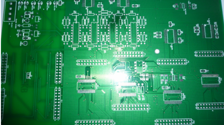
printed circuit board material
The base material of printed circuit board is generally considered to be suitable and the epoxy glass cloth copper clad laminate (FR4) is used. (including single panel)
printed circuit board Copper foil
a. More than 99.9% electrolytic copper;
b. The thickness of copper foil on the surface of the finished double-layer plate shall be no less than 35? M (1oz); if there are special requirements, it shall be specified in the drawings or documents.
printed circuit board structure, dimensions and tolerances
1. Structure
a. The relevant preset elements of printed circuit board should be described in the preset drawing. The appearance should be expressed in mechanical 1 layer or keep out layer. If it is used in the preset file at the same time, the ordinary keep out layer is used for shielding without opening holes, and mechanical 1 is used to express the shape.
b. In the preset pattern, the long slot holes or hollows can be expressed, and the corresponding patterns can be drawn with mechanical 1 layer.
2. Plate thickness tolerance
3. Dimensional tolerance
printed circuit board dimensions shall meet the requirements of preset drawings. When there is no specification in the drawing, the overall dimension tolerance is ± 0.2mm. (V-CUT products are not included)
4. The simplest flatness (warpage) tolerance
The simplest flatness of printed circuit board shall meet the requirements of preset pattern. When there is no regulation in the drawing, the following shall be followed
printed circuit board wire and pad
1. Layout
a. In principle, the layout, thickness and spacing of printed wires and pads shall be in accordance with the provisions of the preset drawings. However, our company will have the following disposal: according to the process requirements, the line width and pad ring width will be reimbursed. If the single panel is ordinary, we will increase pad to enhance the reliability of customer welding.
b. When the preset line spacing can not meet the process requirements (too dense may affect the performance and Manufacturability), our company will conduct proper debugging according to the pre-set specifications.
c. In principle, our company suggests that when customers preset single and double-sided boards, the inner diameter of via should be set above 0.3 mm, the outer diameter should be set above 0.7 mm, the preset line spacing should be 8 mil, and the line width should be more than 8 mil. In order to extremely reduce the production cycle, reduce the difficulty of production.
d. Our minimum drilling tool is 0.3, and the finished hole is about 0.15mm. The minimum line spacing is 6 mil. The thinnest line width is 6 mil. (but the production cycle is longer and the cost is higher)
2. Conductor width tolerance the internal control standard of width tolerance of printed conductor is ± 15%
3. Disposal of grid
a. In order to prevent blistering of copper surface during wave soldering and printed circuit board board buckling due to thermal stress after heating, it is proposed to lay the large copper surface into grid.
b. The grid spacing is ≥ 10mil (no less than 8mil), and the grid width is ≥ 10mil (no less than 8mil).
4. Disposal of thermal pad
In the grounding (electricity) of large plane or object surface, the legs of the components are often connected with them. The disposal of the joint legs takes into account the electrical performance and process requirements, and makes the cruciform pad (heat insulation pad), which greatly reduces the possibility of virtual solder joint sprouting because the profile is not very heat dissipation.
printed circuit board Hole diameter
1. Definition of metallization (PHT) and non metallization (npth)
a. We acquiesce in the following forms of nonmetallic pores:
When the customer sets the nonmetallic property of the mounting hole in Protel99SE advanced properties (remove the plated option in the Advanced menu), our company acquiesces in the nonmetallic hole.
When the customer directly uses the keep out layer or mechanical 1 layer arc to express the hole in the preset file (there is no separate hole), we acquiesce in the nonmetallic hole.
When customers place npth words near the hole, we acquiesce in non metallization of the hole.
When the customer clearly requires the corresponding pore size non metallization (npth) in the preset notice, it shall be disposed according to the customer's requirements.
b. In addition to the above conditions, element holes, mounting holes, through holes, etc. shall be metallized.
2. Bore size and tolerance
a. Preset printed circuit board component holes and mounting holes in the drawing are allowed to be the final pore size of the finished product. The hole diameter tolerance is generally ± 3mil (0.08mm);
b. Through hole (i.e. via hole) is generally controlled as follows: negative tolerance is not required, and positive tolerance is controlled within + 3mil (0.08mm).
3. Thickness
The uniform thickness of copper plating layer of metallized hole is generally not less than 20? M, and the thinnest part is not less than 18? M.
4. Hole wall finish
PTH hole wall finish is generally controlled at ≤ 32um
5. Pin hole problem
a. The pin should be the minimum of 9 mm.
b. When customers have no special requirements, and the preset apertures in the documents are less than 0.9mm, we will add pin holes in the blank wireless path in the board or appropriate positions on the large copper surface.
6. Preset of slot hole (slot hole)
a. It is suggested that the slot hole can be drawn with mechanical 1 layer (keep out layer), or it can be expressed by connecting hole, but the connected hole should have the same volume and the core of the hole should be on the same parallel line.
b. Our minimum slotting cutter is 0.65mm.
c. When the slot hole is used for shielding to prevent creepage between high and low voltage, it is suggested that its diameter should be more than 1.2mm to facilitate processing.
6, Solder mask
1. Coating position and defect
a. Solder mask shall be applied on the surface of printed circuit board except for pad, mark point and test place.
b. If the customer uses fill or track to express the disk, it is necessary to draw the corresponding volume in the solder mask layer