Introduction: PCB is the abbreviation of printed circuit board in English. In general, in the insulation material, according to pre-set, made into printed circuit, printed components or a combination of the two conductive graphics known as printed circuit. And in the insulating substrate to provide electrical bonding between components of the conductive graphics, known as printed circuit. So the printed circuit or printed circuit board is called printed circuit board, also known as printed circuit board or printed circuit.
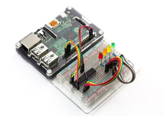
Production technology of PCB printed circuit board
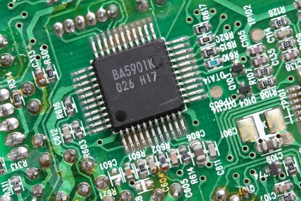
Almost all the facilities we can see from PCB are inseparable from it, ranging from watches, calculators and general-purpose computers on electronic wrists to computers, communications, and military weapon systems. As long as there are no electronic components such as integrated circuits, PCB is needed for their electrical interconnection. It provides mechanical support for various fixed assembly of integrated circuits, successfully realizes wiring and electrical connection or insulation between various electronic components such as integrated circuits, and supplies special electrical properties required, such as special property impedance, etc. At the same time, it provides solder mask graphics for semi-automatic soldering, and provides error identification characters and graphics for component insertion, inspection and maintenance.

How is PCB made?
When we open the keyboard of a general-purpose computer, we can see a piece of soft film (flexible insulating substrate), printed with silver color (silver paste) conductive pattern and healthy position pattern. Because of the general screen leakage method to obtain this pattern, we call this kind of printed circuit board as flexible silver paste printed circuit board.
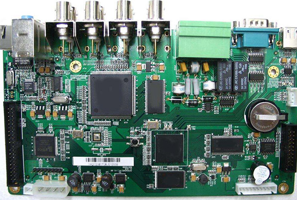
And we go to the computer city to see a variety of computer motherboards, video cards, sound cards and home appliances on the printed circuit board is not the same. The base material is made of paper (usually used on one side) or glass cloth (usually used on both sides and multi layers), pre impregnated with phenolic resin or natural epoxy resin, and then laminated and solidified with copper sheet on one or both sides of the surface layer. This kind of circuit board is covered with copper sheet material, we call it rigid board.
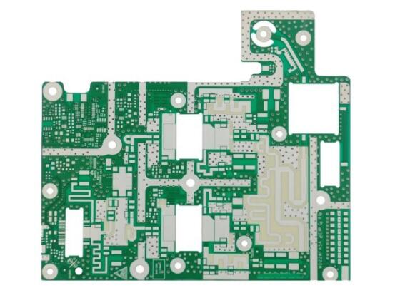
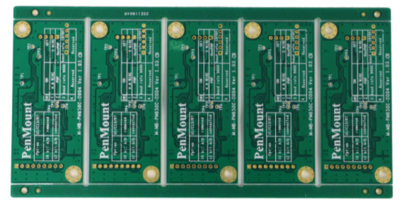
Then made into printed circuit board, we call it rigid printed circuit board. One side has printed circuit graphics, we call it single-sided printed circuit board, two-sided printed circuit graphics, and then through the metallization of holes, the implementation of double-sided interconnection formed printed circuit board, we call it double-sided board. If a printed circuit board with two sides as the inner layer, two single sides as the outer layer or two double sides as the inner layer and two single sides as the outer layer, the printed circuit board which is alternately connected by the positioning system and insulating bonding materials and the conductive patterns are interconnected according to the preset requirements, will become a four layer or six layer printed circuit board, also known as multilayer printed circuit board.
Today, there are more than 100 layers of practical printed circuit boards.
PCB production process is more complex, it involves a wide range of processes, simple methods to deal with single machining to complex machining, there are ordinary chemical reactions, photochemistry, electrochemistry, thermochemistry and other processes, computer aided preset cam and other aspects of knowledge.
And in the production process, there are many process problems and new problems will be encountered from time to time, and the local problems will disappear without finding out the end cause. Because the production process is a non continuous way of plane contact line, no matter what link is wrong, it will lead to the whole line production or large quantity of waste. If the printed circuit board is scrapped by karma, there is no way to recycle it.
Therefore, many engineers left the industry and turned to PCB facilities or material suppliers to do sales and technical services.
Production technology of PCB printed circuit board
In order to advance our understanding of PCB, we have to understand the manufacturing process of general single-sided and ordinary multilayer board, and increase the depth of understanding of it.
Single side rigid printed circuit board: - single side copper clad laminate - blanking - (scrubbing and drying) - drilling or punching - screen printing circuit anti-corrosion pattern or using dry film - curing, checking and repairing board - etching copper - removing anti-corrosion printing material, drying - scrubbing and drying - screen printing solder mask (commonly used green oil), UV curing - screen printing character mark graphics, UV curing - preheating, punching and shape - electrical opening and short circuit Road test - scrubbing and drying - pre coating of welding aid anti oxygen gasifier (drying) or tin spraying hot air leveling - inspection and inspection of packaging - delivery of finished products.
Double sided rigid PCB:
Double sided copper clad laminate - blanking - lamination - digital control drilling through hole - inspection, deburring and scrubbing - electroless plating (through-hole metallization) - (plating thin copper on the whole board) - inspection and cleaning - screen printing negative circuit graphics, curing (dry film or wet film, exposure, development) - inspection and inspection, plate repair - circuit graphics electroplating - tin plating (anti-corrosion nickel / gold) - printing material (sense) Light film) - etch copper - (tin stripping) - cleaning and scrubbing - screen printing solder mask, commonly used heat curing green oil (paste photosensitive dry film or wet film, exposure, development, heat curing, commonly used photosensitive heat curing green oil) - cleaning, drying - screen printing character graphics, curing - (tin spraying or organic solder coating) - appearance processing - cleaning and drying - electrical on-off inspection and measurement - inspection and inspection of package Loading - finished products leaving the factory.
Through hole metallization process flow of multi-layer laminate production - double side cutting of inner layer copper clad laminate - scrubbing - drilling positioning hole - sticking photoresist dry film or coating photoresist - exposure - development - etching and film removal - inner coarsening and deoxidization - inner layer investigation - (outer layer single-sided copper clad laminate circuit manufacturing, b-step bonding sheet, plate bonding sheet checking, positioning hole drilling) - lamination - digital Control drilling - hole inspection - pre hole disposal and electroless copper plating - thin copper plating on the whole board - coating investigation - sticking light resistant electroplating dry film or coating photoresist plating agent - surface layer and bottom plate exposure - development and repair board - circuit graphic electroplating - tin lead alloy or nickel / gold plating - film removal and etching - search and arrest - screen printing solder mask or photo solder mask - printed character graphics - (hot air leveling or Organic solder film) - digital control washing shape - cleaning and drying - electrical on-off inspection and determination - finished product inspection - packaging and delivery.
It can be seen from the process flow chart that the multi-layer plate technology is developed from the foundation of double face metallization process. In addition to the double-sided process, it also has several unique and special internal significance: interconnection of metallized holes, drilling and deoxidizing oxygen drilling, positioning system, lamination and special materials.
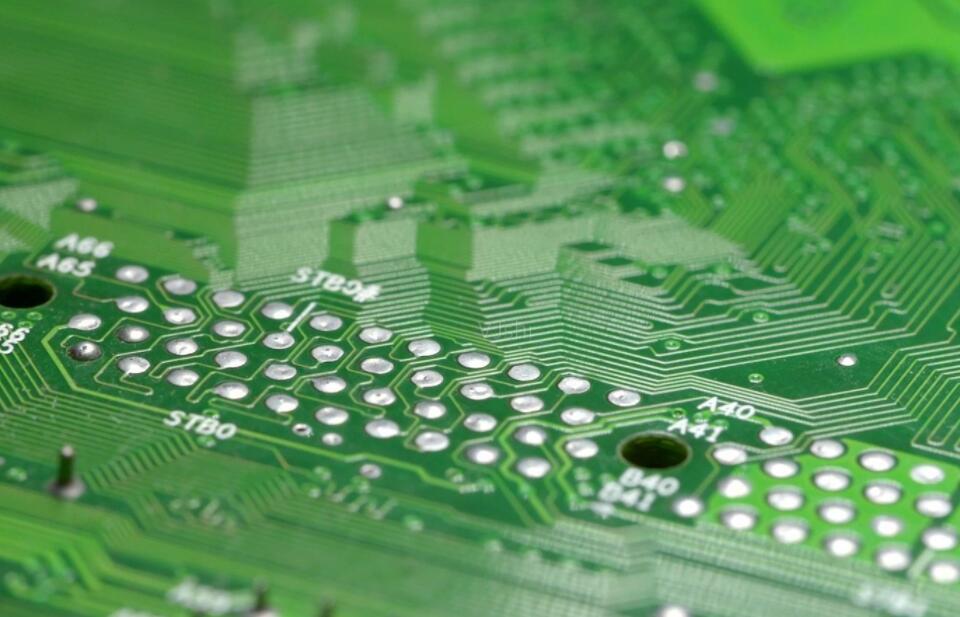
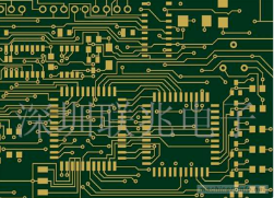
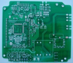
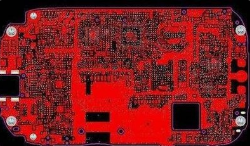
Our common computer boards are basically double-sided printed circuit boards based on epoxy resin glass cloth. There are plug-in components on one side and the soldering surface of component pins on the other side. It can be seen that the solder joints are very regular. The component pins of these solder joints have separate welding surfaces, so we call them pads. Why are other copper wire patterns not tin coated. Due to the need for tin solder pad and other parts, the remaining part of the surface has a layer of wave soldering resistance film. Most of the solder mask on its surface is green color, and a small amount of them are suitable to use yellow, black, blue, etc. Therefore, solder resist oil is often called green oil in PCB industry. The utility of this method is to avoid bridge phenomenon in wave welding, increase welding quality and save solder equivalent. It is also a long-term PCB care layer, can play a moisture-proof, anti-corrosion, mildew and mechanical scratch equivalent. From the outside, the appearance of the bright green color solder mask, film on the plate photosensitive heat curing green oil. Therefore, the appearance of the solder pad is not very accurate.
Exterior mounting technology has the following advantages:
(1) Because of the large number of printed circuit boards, the interconnection technology of large through-hole or buried hole is eliminated, the wiring density on the printed board is increased, the size of printed board plane or object surface is reduced (generally one third of plug-in installation), and the preset layer number and cost of printed circuit board can be reduced.
(2) It has slowed down the weight, increased the seismic performance, considered appropriate and used glue solder, thought of new welding technology, increased the quality and reliability.
(3) Because of the increase of wiring density and the reduction of lead length, the parasitic capacitance and inductance are reduced, which is more helpful to increase the electrical parameters of PCB.
(4) Compared with plug-in installation, it is easier to realize semi-automation successfully, increase installation speed and labor productivity, and reduce assembly cost accordingly.
It can be seen from the above appearance safety technology that the growth of PCB technology is growing with the growth of chip packaging technology and surface mounting technology. Now we look at the computer board, its surface adhesion rate is constantly rising. In fact, this kind of circuit board and transmission screen printing circuit graphics is no way to meet the technical requirements. Therefore, the normal high and very accurate circuit board, its circuit graphics and solder mask patterns are basically considered appropriate, and the use of photosensitive circuit and photosensitive green oil manufacturing process.
With the development of high density PCB, the requirement of PCB production is higher and higher. More and more new technologies are applied to PCB production, such as laser technology, photosensitive natural resin, etc. The above is only a superficial introduction. There are many items in PCB production that are not explained clearly due to space limitation, such as blind buried hole, flexible board, Teflon board, lithography technology, etc. If we want to deepen the discussion, we should try our best.