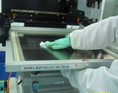
1. Process flow: degreasing - water washing - micro etching - water washing - pickling - pure water washing - OSP - pure water washing - drying.
2. OSP material types: rosin, active resin and azole. The OSP material used in deep connection circuit is azole OSP which is widely used at present.
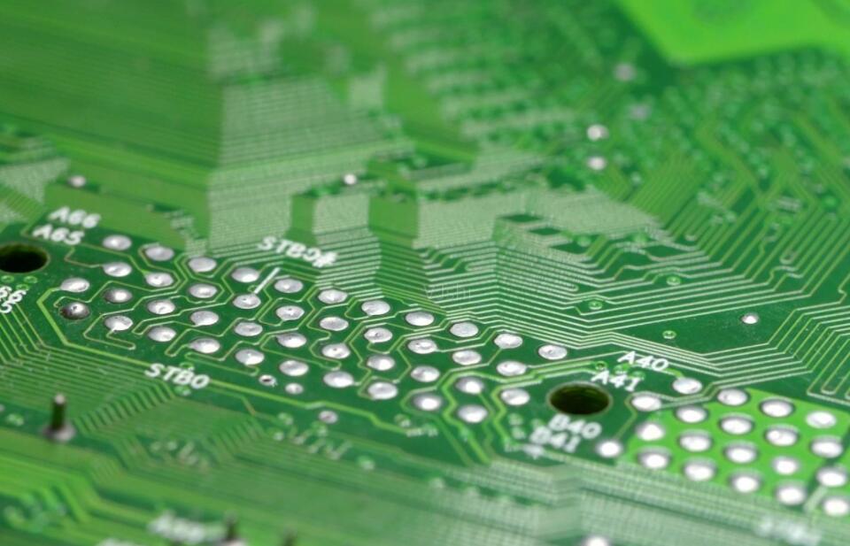
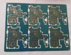
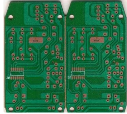
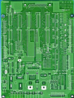
What is the surface treatment process of PCB board OSP
3. Features: good flatness, no IMC formed between OSP film and PCB pad copper, allowing solder and PCB copper to be directly welded (good wettability), low-temperature processing technology, low cost (lower than HASL), less energy consumption during processing, etc. It can be used not only on low-tech PCB, but also on high-density chip packaging substrate. Insufficient points of PCB proofing euguest board: 1. the appearance inspection is difficult, and it is not suitable for multiple reflow soldering (three times are generally required); 2. OSP film surface is easy to scratch; 3. high storage environment requirements; 4. short storage time.
4. Storage method and time: vacuum packaging for 6 months (temperature 15-35 degree Celsius, humidity RH ≤ 60%).
5. SMT site requirements: 1. the OSP circuit board must be stored in low temperature and low humidity (temperature 15-35 degree Celsius, humidity RH ≤ 60%) and avoid exposure to the environment full of acid gas. The assembly of OSP should be started within 48 hours after unpacking; 2. it is recommended to use it within 48 hours after one-sided loading, and it is recommended to store it in low-temperature cabinet instead of vacuum packaging; 3. it is recommended to complete dip within 24 hours after the completion of both sides of SMT.