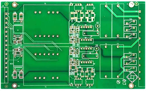
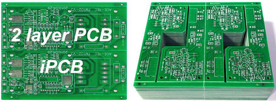
Model: 2 layer PCB
Material: FR4
Material manufacturer: KB, SY, ISOLA
Layer: 2Layer
Color: Green/White/Black
Finished Thickness: 0.15mm - 12mm
Copper Thickness: 1OZ - 6OZ
Surface Treatment: Immersion Gold/OSP/HASL
Application products: power adapter, control panel
2 layer PCB with copper coated on both sides including top and bottom. It is the most common and common PCB circuit board. Both sides of its insulating substrate have conductive graphics, and the electrical connections on both sides are mainly connected through vias or pads. Because both sides can be wired, the difficulty of wiring is greatly reduced, so it is widely used.
There is wiring on both sides of the 2 layer PCB, but to use the wires on both sides, there must be an appropriate circuit connection between the two layers. This "bridge" between circuits is called a pilot hole. The guide hole is a small hole filled or coated with metal on the PCB board, which can be connected with the wires on both sides. Because the area of the double-sided board is twice as large as that of the single panel, the double-sided board solves the difficulty of staggered wiring in the single panel (it can be connected to the other side through holes), and it is more suitable for more complex circuits than the single panel.

2 layer PCB
Difference between 2 layer PCB vs 4 layer PCB in SMT processing
2 layer PCB
Compared with 4 layer PCB board, a double-sided PCB board is easier to use because of its simple design. Although not as simple as a single panel, they are as simple as possible without sacrificing the two-sided input function. The reduced complexity leads to the same reduced price tag, but this means that it is less likely than a four-layer PCB board. However, as the most commonly used circuit board in the industry, its significant advantage is that there is no signal propagation delay.
4 layer PCB
The four-layer board PCB has a larger surface area than the double-sided PCB board, which increases the possibility of more wiring. Therefore, they are very suitable for more complex equipment. Because of their complexity, production costs will be higher and development will be slower. They are also more likely to have propagation delay or mutual influence, so reasonable design is very important.
2 layer PCB design rules - via and pad
Via is called through-hole, which can be divided into through hole, blind hole, and buried hole. It is mainly used for the connection of wires in different layers of the network. It can not be used as a plug-in hole welding element. Via hole diameter is not controlled during production.
Pad is can be divided into a pin pad and surface bonding pad. The pin pad has a welding hole, which is mainly used for welding pin components. The surface bonding pad has no welding hole and is mainly used for welding surface bonding components.
The diameter of the pad hole shall be controlled during production, with a tolerance of plus or minus 0.08mm.
Via mainly plays the role of electrical connection. In actual production, it may compensate to increase the hole and close hole knife production, reduce the number of knives and improve work efficiency, or reduce the aperture due to the limited line spacing and linewidth space to meet the production requirements.
The aperture of via is generally small, which is usually sufficient as long as the plate-making process can be achieved. Via surface can be coated with solder resist ink or not; The pad not only plays the role of electrical connection but also plays the role of mechanical fixation. The aperture of the pad must be large enough to pass through the pins of the components, otherwise, it will lead to production problems; In addition, the pad surface must not have solder resist ink, because it will affect the welding. The hole tolerance shall be controlled to be plus or minus 0.08mm or large or small. This will result in a loose installation.

2 layer PCB
2 layer PCB manufacturing process
Two-sided PCB copper clad sheet cutting, one drill reference hole, one numerical control drill through-hole one test, one deburring one brushing one electroless plating (metallization of through-hole) one full plate electroplating thin copper one test brushing one screen print negative circuit graphics, solidification (dry or wet film, exposure, development) one test, First-line pattern of trimming board electroplating one electroplating tin (anti-corrosive nickel/gold), one printing material (photo film), one etching copper and one tin removal one cleaning brushing one screen printing solder graphic (dry or wet film, exposure, development, heat curing, commonly used photo-thermal curing green oil) - cleaning, drying one screen printing marker character graphic, curing one shape processing, cleaning, etc. In drying and electrical break test a tin spray or organic bonding film a test package finished product factory.
The quality control of electroplated copper layer on 2 layer through-hole printed circuit board is very important, because the development of multi-layer or multi-layer board to high density, high precision, and multi-function requires more and more stringent binding force, uniform fineness, tensile strength, and elongation of the copper-plated layer, so the quality control of electroplating on through-hole printed circuit board is especially important.
To ensure the uniformity and consistency of 2 layer PCB copper plating layer, most of the copper plating processes for high aspect ratio printed circuit boards are assisted by high-quality additives, combined with moderate air stirring and cathode movement, under relatively low current density conditions, so that the control area of electrode reaction in the hole is enlarged, and the role of electroplating additives can be displayed. In addition, the cathode movement is very helpful to improve the deep plating ability of the plating solution, increase the polarization of the plated parts, and compensate the formation rate of crystal nuclei and the growth rate of crystals during the electrocrystallization process of the plating layer, thus obtaining a high-toughness copper layer.
Of course, the current density is set according to the actual plating area of the 2 layer PCB. From the electroplating principle, the value of current density must also depend on the main salt concentration, solution temperature, additive content, and stirring degree of high acid and low copper electrolyte. In a word, the technological parameters and conditions of copper plating must be strictly controlled in order to ensure that the thickness of the copper-plated layer in the hole conforms to the technical standards.
IPCB company is a professional PCB circuit board manufacturer. We can mass produce 2-layer PCB at low 2 layer PCB cost, so we provide cheap 2 layer PCB.
Model: 2 layer PCB
Material: FR4
Material manufacturer: KB, SY, ISOLA
Layer: 2Layer
Color: Green/White/Black
Finished Thickness: 0.15mm - 12mm
Copper Thickness: 1OZ - 6OZ
Surface Treatment: Immersion Gold/OSP/HASL
Application products: power adapter, control panel
For PCB technical problems, iPCB knowledgeable support team is here to help you with every step. You can also request PCB quotation here. Please contact E-mail sales@ipcb.com
We will respond very quickly.