The most reliable PCB & PCBA custom service factory.
Language

Language
PCB copying board has no software , so it can only be measured and drawn with caliper edge, and it’s very slow and its accuracy is also poor. However, It is very easy to copy the board with the software. Generally, it is more convenient to use the board copying software of delta company. You can scan or take a picture of the PCB board first, and then load the picture into the software according to the gourd drawing ladle. But it’s more difficult to transform the PCB diagram into schematic diagram, because it needs experience and knowledge, otherwise, it can’t be completed successfully.
It is more troublesome to copy the multi-layer board, because the inner layer cannot be seen, so we can only damage the sample. Generally, we cope on the top and bottom first, and then keep the bottom and the top down in front of the photo (for reference). Beside, a accurate method is to dismantle all components, and then register all components parameters, and number one by one of the components and silkscreen layer corresponding to retain the original information, or scan again to bare PCB photography, get photos or scan in software. Different software has different requirements, like the size of photo, if the size is too big, it will have a effect on the the speed of copy board. So too big PCB copy board can be divided into several small pieces, then split. After the upper and lower layers are completed, the finished layer can be polished with sandpaper to gradually expose the inner layer, copy one layer and then grind the next layer until all is completed.
Need scanners, computers, PORTEL99 and AUTOCAD
This is a relatively complex process, the details need to consult relevant professionals
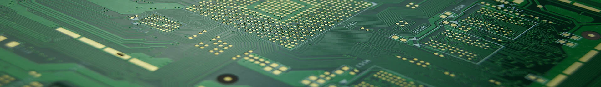
What are the steps of PCB copying? The technical realization process of PCB copying is simply to scan the circuit board to be copied, record the detailed position of the components, and then remove the components to make a bill of materials (BOM). ) And arrange the purchase of materials. The blank board is scanned into a picture and processed by the copying software to restore it to a PCB board drawing file, and then the PCB file is sent to the plate making factory to make the board. After the board is made, the purchased components are welded to the made On the PCB board, then go through the circuit board test and debugging.
What are the steps of PCB board copying?
Get a piece of PCB, first record the model, parameters, and position of all vital parts on the paper, especially the direction of the diode, the tertiary tube, and the direction of the IC gap. It is best to use a digital camera to take two photos of the location of the vital parts. The current PCB circuit boards are getting more and more advanced. Some of the diode transistors on the above are not noticed and can't be seen at all.
Remove all the multi-layer boards and copy the boards, and remove the tin in the PAD hole. Clean the PCB with alcohol and put it in the scanner. When the scanner scans, you need to raise the scanned pixels slightly to get a clearer image. Then lightly polish the top and bottom layers with water gauze until the copper film is shiny, put them in the scanner, start PHOTOSHOP, and scan the two layers in separately in color. Note that the PCB must be placed horizontally and vertically in the scanner, otherwise the scanned image cannot be used.
Adjust the contrast and brightness of the canvas so that the part with copper film and the part without copper film have a strong contrast, and then turn the second image into black and white, and check whether the lines are clear. If not, repeat this step. If it is clear, save the picture as black and white BMP format files TOP.BMP and BOT.BMP. If you find any problems with the picture, you can use PHOTOSHOP to repair and correct it.
Convert the two BMP format files to PROTEL format files, and transfer them into two layers in PROTEL. For example, the positions of PAD and VIA that have passed through two layers basically coincide, indicating that the previous steps have been done well. Repeat the third step. Therefore, PCB copying is a job that requires patience, because a small problem will affect the quality and the degree of matching after copying the board.
Convert the two BMP format files to PROTEL format files, and transfer them into two layers in PROTEL. For example, the positions of PAD and VIA that have passed through the two layers basically coincide, indicating that the previous steps have been done well. If there is a deviation, then Repeat the third step. Therefore, PCB copying is a job that requires patience, because a small problem will affect the quality and the degree of matching after copying the board.
Import TOP.PCB and BOT.PCB in PROTEL and combine them into one picture and it will be OK.
Use a laser printer to print TOP LAYER and BOTTOM LAYER on transparent film (1:1 ratio), put the film on the PCB board, and compare whether there is any error. If it is correct, you are done.


