The most reliable PCB & PCBA custom service factory.
Language

Language
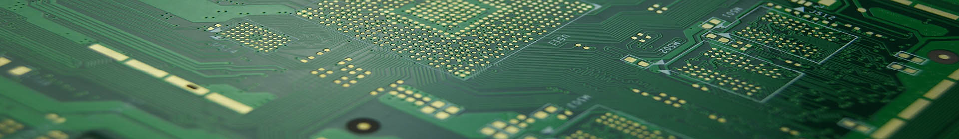
Via is one of the important components of multi-layer PCB, and the cost of drilling usually accounts for 30% to 40% of PCB manufacturing cost. Simply put, every hole on the PCB can be called a via. From the point of view of function, vias can be divided into two categories: one is used for electrical connections between layers; the other is used for fixing or positioning devices. In terms of process, these vias are generally divided into three categories, namely blind vias, buried vias and through vias. Blind vias are located on the top and bottom surfaces of the printed circuit board and have a certain depth. They are used to connect the surface line and the underlying inner line. The depth of the hole usually does not exceed a certain ratio (aperture). Buried hole refers to the connection hole located in the inner layer of the printed circuit board, which does not extend to the surface of the circuit board. The above-mentioned two types of holes are located in the inner layer of the circuit board, and are completed by a through-hole forming process before lamination, and several inner layers may be overlapped during the formation of the via. The third type is called a through hole, which penetrates the entire circuit board and can be used for internal interconnection or as a component mounting positioning hole. Because the through hole is easier to implement in the process and the cost is lower, most of the printed circuit boards use it instead of the other two types of through holes.
Let's start with traditional laminates.The standard multi-layer circuit board structure is composed of inner and outer layer, and the inner connection function of each layer circuit is achieved through drilling and metallization.However, due to the increase of line density, the packaging method of parts is constantly updated.In order to allow the limited circuit board area to accommodate more parts with higher performance, in addition to the thinner line width, the aperture is also reduced from 1 mm of DIP jack aperture to 0.6 mm of SMD, and further reduced to less than 0.4mm.However, it will still occupy the surface area, so there are buried holes and blind holes.
Buried holes and blind holes are defined as follows:
A. Buried Via
The through hole between the inner layer, after pressing, can not be seen, so do not occupy the outer area, the upper and lower sides of the hole are in the internal layer of the PCB, in other words, buried in the PCB.
B. Blind Via
Applied to the communication of a surface layer and one or more inner layers, one side of the hole is on the side of the PCB, and then passes to the inside of the board.
Through Hole: Plating Through Hole is abbreviated as PTH. This is the most common one. You only need to pick up the PCB and face the light, and the holes that can see the light are "through holes". This is also the simplest type of hole, because when making it, you only need to use a drill or a laser to directly drill the circuit board, and the cost is relatively cheap. But on the other hand, some circuit layers do not need to connect these through holes. For example, we have a six-story house. I bought its third and fourth floors. I want to design a staircase inside that only connects the third floor to the third floor. It's fine between the fourth floor. For me, the space on the fourth floor is invisibly used up by the original staircase connecting the first floor to the sixth floor. So although through holes are cheap, they sometimes use up more PCB space.
Blind Hole: Blind Via Hole. Blind vias refer to vias that connect the inner layers and are not visible on the surface of the finished board. The above-mentioned two types of holes are located in the inner layer of the circuit board, and are completed by a through-hole forming process before lamination, and several inner layers may be overlapped during the formation of the via.
The outermost circuit of the PCB is connected with the adjacent inner layer by plating holes. Because the opposite side cannot be seen, it is called "blind pass". In order to increase the space utilization of the PCB circuit layer, a "blind via" process has emerged. This production method requires special attention to the depth of the drilling (Z axis) to be just right. This method often causes difficulties in electroplating in the hole, so it is almost used by no manufacturer: it is also possible to place the circuit layer that needs to be connected in the individual circuit layer in advance. At that time, the holes should be drilled first, and then glued together, but a more precise positioning and alignment device is required.
Buried hole: Buried hole PCB internal connection of any circuit layer but not conducted to the outer layer. This process cannot be achieved by drilling after bonding. It must be drilled at the time of individual circuit layers. After the inner layer is partially bonded, it must be electroplated before it can be fully bonded. Compared with the original "through hole" and "Blind holes" take more time, so the price is the most expensive. This process is usually only used for high-density (HDI) circuit boards to increase the usable space of other circuit layers.


