The most reliable PCB & PCBA custom service factory.
Language

Language
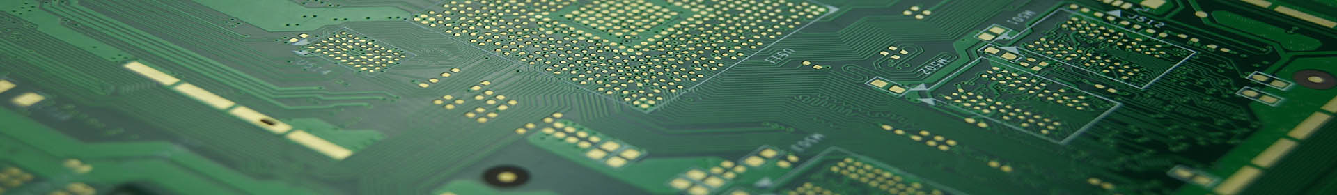
The PCB HASL process, also called Hot air solder leveling, is an important process in PCB fabricatiaon. The PCB HASL process mainly includes lead-free tin spraying and lead-free tin spraying. These two types of processes are also commonly used. It is widely used in PCB manufacturers. The quality of tin spraying directly affects the quality of subsequent customers' soldering. Therefore, tin spraying has become the focus of quality control of PCB manufacturers. The characteristics of PCB tin spraying types and related basic knowledge are introduced below.
The HASL PCB board is a common type of PCB board, generally a multi-layer PCB(4-46 layer) high-precision PCB board, used in various electronic equipment, communication products, computers, medical equipment, aerospace and other fields and products Will be used in.
The HASL PCB is to soak the PCB in molten tin and lead. When enough tin and lead is attached to the surface of the PCB, hot air pressure is used to scrape off the excess tin and lead. After the tin-lead is cooled, the soldered area of the PCB will be stained with a layer of tin-lead with an appropriate thickness. This is the general procedure of the tin-spraying process. The surface treatment technology of PCB, currently the most widely used is the spray tin process, also called hot air leveling technology, which sprays a layer of tin on the pad to enhance the conduction performance and solderability of the PCB pad.
As the most common form of surface coating for PCB board surface treatment, PCB tin spraying process is widely used in the production of circuits. The quality of tin spraying will directly affect the quality of soldering and soldering during subsequent customer production. sex. Therefore, the quality of tin spraying has become a key point of quality control for PCB manufacturers. For general double-sided PCB boards, tin spraying and OSP processes are the most used, while rosin technology is widely used on single-sided PCBs, and gold-plating technology is used for ICs that need to be bonded On the PCB. Immersion gold is used more on plug-in boards.
Hot air solder leveling (Hot air solder leveling) is a step and process in the production process of PCB board. Specifically, the PCB boards are immersed in a molten solder pool, so that all exposed copper surfaces will be covered by solder. Then use a hot air cutter to remove the excess solder on the PCB board. Because the surface of the PCB after tin spraying is the same substance as the solder paste, the soldering strength and reliability are better. However, due to its processing characteristics, the surface flatness of the spray tin treatment is not good, especially for small electronic components such as BGA package types. Due to the small soldering area, if the flatness is not good, it may cause problems such as short circuits, so flatness is required. A better process to solve the problem of tin spraying board. Generally, the gold-plating process is selected (note that it is not a gold-plating process), and the principle and method of chemical displacement reaction are used for reprocessing, and a nickel layer with a thickness of 0.03~0.05um or about 6um is added to improve the surface flatness.
Advantages of HASL PCB Board
1. The wettability is better during the soldering process of the components, and the soldering is easier.
2. It can prevent the exposed copper surface from being corroded or oxidized.
Product shortcomings Voice
1. The flatness at the vertical level is poor, and it is not suitable for the welding and use of fine-pitch components. The flatness can be improved by increasing the horizontal level.
2. The high thermal stress during processing may damage the PCB board and cause flaws or defects.
The role and process flow of HASL PCB Board
The PCB spray tin process is mainly: placing the board (sticking with gold-plated plug protection tape)-pre-treatment of hot air leveling-hot air leveling-cleaning after hot air leveling-inspection.
Although the overall process of HASL PCB Board is simple, there are still many process conditions that need to be mastered if you want to flatten a good and qualified printed PCB with hot air, such as: solder temperature, air knife air temperature, air knife pressure, dipping time, and increase Speed and so on. These conditions have set values, but they must be changed according to the external conditions of the printed PCB and the requirements of the processing order when working, such as: board thickness and board length. Different single-sided, double-sided, and multi-layer boards. The conditions they use are different. Only by familiarizing and mastering various process parameters, according to the different types of printed PCBs, different requirements, patience, meticulous, and reasonable adjustment of the machine, can the hot air flatten a qualified printed PCB.
The main function of HASL PCB Board
(1) Prevent oxidation of the bare copper surface; copper is easily oxidized in the air, causing the PCB pad to be non-conducting or reducing the soldering performance. By applying tin on the copper surface, the copper surface can be effectively isolated from the air and keep the PCB Continuity and solderability.
(2) Maintain solderability; other surface treatment methods include: hot melt, organic protective film OSP, chemical tin, chemical silver, chemical nickel gold, electroplated nickel gold, etc.; but the cost-effective price of tin spraying board is best to spray tin Process characteristics of PCB board The sprayed tin board includes two layers of copper and tin, which can adapt to poor environmental conditions and the soldering performance is better. It is more suitable for high temperature and corrosive environments.
This kind of PCB board is commonly used in industrial control equipment communication products and military equipment products. The advantages of tin-spraying PCB: in the usual PCB surface treatment, the tin-spraying process is called the best solderability, because there are already on the pads Tin, when soldering tin, it is easier with gold-plated board or rosin and OSP process. This is very easy for us to solder by hand, and soldering is very easy.
Features of HASL PCB Board
HASL PCB Board is the most commonly used process, this process is more practical, it has good welding performance, has a good anti-oxidation effect, and the price is relatively affordable, and a very cost-effective process. The HASL PCB Board also has two distinctions: lead-free and lead-free:
1. Lead-free HASL PCB Board
Lead-free tin is an environmentally friendly process. It has very little harm to the human body. It is also a process advocated at this stage. The content of lead in lead-free tin does not exceed 0.5. Lead-free tin has a high melting point, so that the solder joints are firm. a lot of. In essence, lead spray tin and lead-free tin spray are a process. It's just that the purity of lead is different. Lead-free tin is more environmentally friendly and safer for the human body, and it is also a future development trend. It is recommended that you use it.
Introduced the characteristics and shortcomings of the two process types, lead spray tin and lead-free tin spray. Among them, lead spray tin is easier to use, but it is not safe, environmentally friendly, and harmful to the human body, so lead-free is recommended Tin spraying is non-toxic and harmless, and it is also a surface treatment process that is currently advocated.
2. Leaded HASL PCB Board
The so-called lead-sprayed tin refers to the tin in a certain proportion, and the lead will increase the activity of the tin wire during the soldering process. The lead-tin wire is better than the lead-free tin wire, but lead is poisonous and contains lead. The lead is harmful to the human body; the eutectic temperature of lead is lower than that of lead-free. How much depends on the composition of the lead-free alloy. For example, the eutectic of SNAGCU is 217 degrees, and the welding temperature is the eutectic temperature plus 30-50 degrees. It depends on actual adjustments. The leaded eutectic is 183 degrees. Lead is better than lead-free in mechanical strength and brightness. Therefore, it is not environmentally friendly to have lead and tin, and it is somewhat different from the environmental protection advocated by the world. Therefore, lead-free tin spray was born.
Distinguish between lead and lead-free
Take a piece of white paper and gently wipe the tin position, the black part is the lead spray tin.


