The most reliable PCB & PCBA custom service factory.
Language

Language
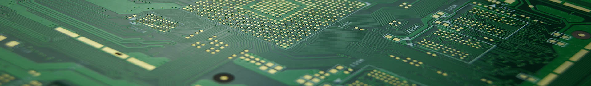
Buried and blind hole pcb board is not necessarily HDI PCB, HDI PCB has a blind hole, buried hole is not necessarily, depending on your product is a few stages of several pressure products.
Explain the following:
6 layer PCB 1+N+1, 2+N+2 is for the demand of laser drilling wrench, that is the HDI PCB.
Finger blind hole of 1+N+1 HDI on 6 layers: 1-2, 2-5, 5-6, namely 1-2, 5-6 requires laser drilling.
Finger blind hole of 6-layer second-order HDI : 1-2, 2-3, 3-4, 4-5, 5-6. Laser drilling is required for 2 times.First, the buried hole of 3-4 was drilled, and the laser hole of 2-3, 4-5 was pressed, and the second laser hole of 1-3, 4-5 was pressed, and the second laser hole of 1-2, 5-6 was drilled, and finally the hole was drilled through. Thus it can be seen that the 2+N+2 HDI was pressed twice, and the laser hole was drilled twice.
One side of the Blind Via PCB is on the surface of the PCB, and then it leads to the inside of the PCB. Blind vias are vias that connect the surface layer and the inner layer without penetrating the entire board. Blind vias refer to vias that connect the inner layers and are not visible on the surface of the finished PCB. The above-mentioned two types of holes are located in the inner layer of the PCB, and are completed by a through-hole forming process before lamination, and several inner layers may be overlapped during the formation of the via.
Buried-hole PCB refers to the inner layer via hole, the surface and bottom layers are invisible, and it is used for the inner layer signal interconnection. Generally used on mobile phones and PDA boards. Buried vias can reduce the probability of signal interference, maintain the continuity of the characteristic impedance of the transmission line, and save wiring space, which is suitable for HDI PCB design. However, HDI PC processing costs are also very expensive, and the new drilling process will solve this problem.
With the development of electronic products to high density and high precision, the same requirements are put forward on PCBs accordingly. The most effective way to increase PCB density is to reduce the number of through holes, and accurately set blind holes and buried holes.
Blind and buried via PCB basic
1. The degree of overlap between layers in the manufacturing of blind and buried multi-layer PCB
By adopting the pin front positioning system of ordinary multi-layer PCB production, the graphic production of each layer of single chip is unified into a positioning system, which creates conditions for the realization of successful manufacturing. For the ultra-thick single chip used this time, if the board thickness reaches 2 mm, a certain thickness layer can be milled at the location of the positioning hole, and it is also attributed to the processing of the four-slot positioning hole punching equipment of the front positioning system Ability.
2. The problem of glue flow on the board surface after PCB lamination
In view of the characteristics of blind and buried multi-layer PCB manufacturing, the use of the process selected by the manufacturing research institute will inevitably cause glue flow on both sides of the PCB after lamination. In order to ensure the graphics transfer accuracy of the following processes and the bonding force requirements of electroplating, manual methods are required to remove the glue on the board surface. This process is relatively difficult and brings inconvenience to the operator. For this reason, when laminating the board, we chose two materials as the release isolation material, one is the currently used polyester film, and the other is the polytetrafluoroethylene film. After comparison experiments, the results show that: the surface flow of the laminate using PTFE film as the release isolation material is significantly better than that of the laminate using polyester film as the release isolation material. This also provides a reference for solving such problems in the future.
3. The position accuracy and coincidence of graphics transfer
As we all know, in accordance with the common practice in the industry, in this blind and buried via multilayer PCB manufacturing process, for the production of each inner layer pattern, we use a silver salt template, which is punched through four holes consistent with the single-chip positioning hole. Slot positioning hole for graphics transfer. In view of the fact that before each inner layer graphics are transferred and produced, each inner layer board is made by numerical control drilling and hole metallization, so there is a protection problem of a four-slot positioning hole. In addition, after the lamination is completed, when the outer layer graphics are transferred, the following methods can usually be used:
A. The diazo film template copied by the silver salt film template is conventionally used, and the two sides are respectively aligned with the fabrication PCB;
B. Use the original silver salt sheet template to locate the fabric PCB according to the four-slot positioning hole;
C. When making the template, while designing the four-slot positioning hole, design two positioning holes outside the effective area of the figure. Then when the outer layer pattern is transferred, the outer layer pattern is used to locate the fabrication PCB through the two positioning holes.
The above three methods have their own advantages and disadvantages. In order to ensure the degree of overlap between layers, some have the problem of protecting the four-slot positioning holes at different stages during the PCB manufacturing process; some have problems with the concentricity of the two-sided graphics after the center is milled during the milling process; some have the layer The asymmetry of the center of the graphics on both sides caused by the pressure factor and the borehole offset.


