The most reliable PCB & PCBA custom service factory.
Language

Language
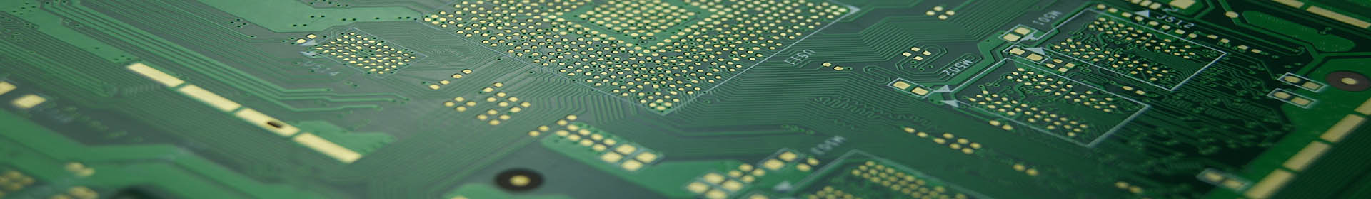
When it comes to PCB, many friends will think that it can be seen everywhere around us, from all kinds of household appliances, computer accessories, to all kinds of digital products, as long as electronic products almost all use PCB, then what is PCB? PCB is printed circuit board, that is printed circuit board, for electronic components to insert, with circuit base plate. The copper plated substrate is printed with anti-corrosion circuit by printing, and then etched to wash out the circuit.

Use the role of the ground pcb layer:
Adding grounding layers to PCB is a very simple, low-cost, and efficient way to design electronic devices with better signal integrity, higher accuracy, and stronger interference resistance.If you are not comfortable , be sure to keep these benefits in mind when laying out the next PCB.
How is the difference distribution line realized?
Two points should be paid attention to in the wiring of differential pairs. One is that the length of the two lines should be as long as possible. The other is that the distance between the two lines (which is determined by the differential impedance) should always remain unchanged, that is, to keep parallel. There are two ways of parallel: one is that two lines run on the same side by side, and the other is that two lines run on two adjacent layers (over under). Generally, there are many ways to implement the former side by side.
For a clock signal line with only one output, how to realize the difference distribution line?
Only when the difference distribution line is used is the signal source and receiver are also differential signals. Therefore, the difference distribution line cannot be used for clock signal with only one output.
Can a matching resistance be added between the differential pairs at the receiving end?
The matching resistance between differential pairs at the receiving end is usually added, and its value should be equal to the value of differential impedance. So the signal quality will be better.
Why do differential pair routing be close and parallel?
The routing of differential pairs should be appropriately close and parallel. The so-called appropriate approach is because the distance will affect the value of differential impedance, which is an important parameter in the design of differential pairs. Parallel is also necessary because of the consistency of differential impedance. If the two lines are far or near, the differential impedance will be inconsistent, which will affect the signal integrity and timing delay.
The power layer in the PCB four-layer board defaults to the network "VCC", and the ground layer defaults to the network "GND". If there is no corresponding network, the network must be set up, so that the layer exists as a flat copper clad layer. When the pins or vias of the same network pass through the circuit board, they are automatically connected to this layer, and different networks will not be connected.
1. PCB (Printed Circuit Board), the Chinese name is printed circuit board, also known as printed circuit board. It is an important electronic component, a support for electronic components, and a carrier for electrical connection of electronic components. Because it is made by electronic printing, it is called a printed circuit board.
2. PCB raw materials
From the beginning of the 20th century to the end of the 1940s, it was the embryonic stage of the development of the PCB substrate material industry. Its development characteristics are mainly manifested in: During this period, resins, reinforcing materials and insulating substrates used for substrate materials have emerged in large numbers, and preliminary explorations have been made in technology. These have created the necessary conditions for the advent and development of copper clad laminates, the most typical substrate material used for printed circuit boards. On the other hand, PCB manufacturing technology, which uses metal foil etching (subtractive method) to manufacture circuits as the mainstream, has been initially established and developed. It plays a decisive role in the determination of the structural composition and characteristic conditions of the copper clad laminate.
PCB polychlorinated biphenyls is a synthetic organic compound used commercially in North America from 1929 to the late 1970s. Although Canada has not processed and produced this chemical substance, it has been widely used in electrical equipment insulation, heat exchangers, etc. In water conservancy systems and other special applications.
It was only decades later that people realized the pollution of PCBs to the global environment. It is a mixture of various chlorinated biphenyls, which is extremely harmful to the human body. The Canadian government has taken measures to try to eliminate PCBs, but the illegal import, processing and sale of PCBs occurred in Canada in 1977, and the PCBs were illegally released into the natural environment in 1985, and the Canadian constitution allows PCB equipment owners to continue to use them. PCB until the life of the equipment. It was only in 1988 that Canadian provincial governments began to regulate the storage, transportation and destruction of PCBs.


