The most reliable PCB & PCBA custom service factory.
Language

Language
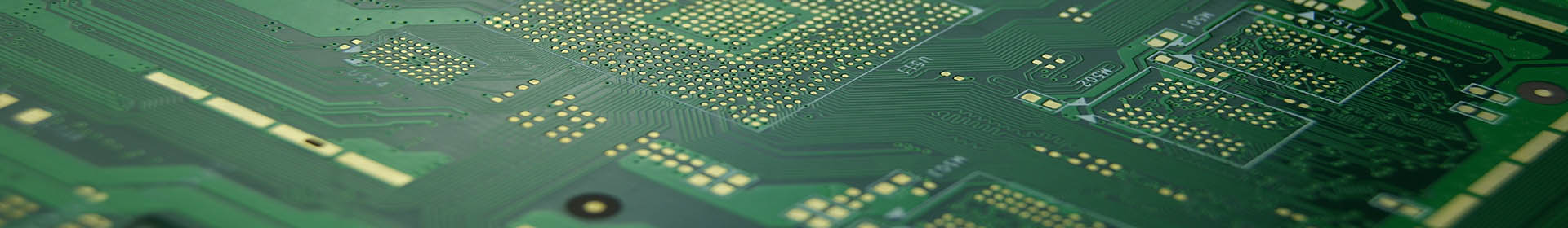
Radio frequency PCB and RF PCB design has a lot of uncertainty in the current published theory, which is often described as a kind of "black art". Generally, for circuits below microwave frequency band (including low-frequency and low-frequency digital circuits), careful planning under the premise of fully mastering various design principles is the guarantee of one-time successful design. For PC digital circuits with microwave frequency band and high frequency, 2 ~ 3 versions of PCB are required to ensure the circuit quality. For RF circuits above microwave band, more versions of PCB design and continuous improvement are needed, and under the premise of considerable experience. From this we can see the difficulties in RF electrical design.

Interference between digital circuit module and analog circuit module
If analog (RF) and digital circuits work separately, they may work well. However, once they are put on the same PCB and work with the same power supply, the whole system is likely to be unstable. This is mainly due to the fact that digital signals frequently oscillate between the ground and the positive source (> 3 V), and the period is particularly short, often nanosecond. Due to the large amplitude and short switching time, these digital signals contain a large number of high frequency components independent of the switching frequency. In the analog part, the signal from the wireless tuning loop to the receiving part of the wireless device is generally less than 1 μ v. Therefore, the difference between digital signal and RF signal can reach 120dB. Obviously, if the digital signal and the RF signal can not be separated well, the weak RF signal may be damaged, so the working performance of the wireless device will deteriorate, or even can not work at all.
Noise interference of power supply
RF circuit is very sensitive to power noise, especially to burr voltage and other high frequency harmonics. Microcontrollers will suddenly absorb most of the current in a short period of time in each internal clock cycle. This is because modern microcontrollers are made in CMOS technology. Therefore, suppose a microcontroller operates at an internal clock frequency of 1MHz, which will extract current from the power supply. If the power supply is not decoupled properly, it will cause voltage burr on the power line. If the voltage burr reaches the power pin of RF part of the circuit, it may lead to work failure.
Unreasonable ground wire
If the ground wire of RF PCB is not handled properly, some strange phenomena may occur. For digital circuit design, even if there is no ground layer, most digital circuit functions well. In the RF band, even a very short ground wire acts like an inductor. Roughly calculated, the inductance per millimeter length is about 1NH, and the inductance reactance of 10mm PCB line is about 27 Ω at 433MHz. If the ground layer is not used, most ground wires will be longer and the circuit will not have the design characteristics.
Radiation interference of antenna to other analog circuit parts
In PCB circuit design, there are usually other analog circuits on the board. For example, many circuits have analog to digital conversion (ADC) or digital to analog converter (DAC). The high frequency signal from the antenna of the RF transmitter may reach the analog input of the ADC. Because any circuit line can send or receive RF signal like an antenna. If the processing of ADC input is not reasonable, RF signal may self excite in ESD diode of ADC input, which will cause ADC deviation.
Design principle and scheme of RF PCB
RF concept layout
In the design of RF layout, the following general principles must be given priority to:
(1) The high-power RF amplifier (HPA) and low-noise amplifier (LNA) should be isolated as far as possible. In short, the high-power RF transmitting circuit should be far away from the low-power RF receiving circuit;
(2) Make sure that there is at least one whole area in the high power area of PCB board, and it is better to have no vias on it. Of course, the larger the copper foil area, the better;
(3) Decoupling of circuit and power supply is also very important;
(4) RF output usually needs to be away from RF input;
(5) Sensitive analog signals should be kept away from high-speed digital signals and RF signals as far as possible.
Design principles of physical and electrical zoning
Design zoning can be decomposed into physical and electrical partitions. The physical partition mainly involves the layout, direction and shielding of components; the electrical partition can be further divided into power distribution, RF wiring, sensitive circuit and signal, grounding, etc.
Physical partition principle
(1) Principle of component location layout. Component layout is the key to achieve an excellent RF design. The most effective technology is to fix the components on the RF path and adjust its direction, so as to minimize the length of the RF path, make the input far away from the output, and separate the high-power circuit from the low-power circuit as far as possible.
(2) PCB stack design principle. The most effective method of circuit board stacking is to arrange the main ground (main ground) in the second layer below the surface layer, and lay the RF line on the surface layer as much as possible. By minimizing the via size on the RF path, not only can the path inductance be reduced, but also the false solder joints on the main ground can be reduced, and the chance of RF energy leakage to other areas in the laminate can be reduced.
(3) RF devices and RF wiring layout principles. In physical space, linear circuits such as multistage amplifiers are usually sufficient to isolate multiple RF regions from each other, but duplexers, mixers, and if Amplifiers / mixers always have multiple RF / if signals interfering with each other, so this effect must be carefully minimized. RF and if traces should be crossed as far as possible, and a piece of ground should be separated between them as much as possible. The correct RF path is very important to the performance of the whole PCB, which is why component layout usually takes up most of the time in the design of cellular phone PCB.
(4) The design principle of reducing the interference coupling of high / low power devices. On a cellular phone PCB, it is usually possible to reduce the noise by placing the amplifier circuit on one side of the PCB, and placing the high-power amplifier on the other side, and finally connecting them on the same side to the antenna at the RF end and baseband processor end through the duplexer. To ensure that through holes do not transfer RF energy from one side of the board to the other, a common technique is to use blind holes on both sides. Through holes can be arranged in the area where both sides of PCB are free from RF interference to minimize the adverse effects of through holes.
Electrical zoning principle
(1) Power transmission principle. Most circuits in cellular phones have relatively small DC currents, so wiring width is usually not a problem. However, a large current line as wide as possible must be provided for the power supply of the high power amplifier to minimize the transmission voltage drop. In order to avoid too much current loss, multiple through holes are needed to transfer current from one layer to another.
(2) Power decoupling of high power devices. If the power supply pin of HPA cannot be fully decoupled, the high-power noise will radiate to the whole board and bring multiple problems. The grounding of high power amplifier is very important, so it is necessary to design a metal shield for it.
(3) RF input / output isolation principle. In most cases, it is also critical to ensure that the RF output is away from the RF input. This also applies to amplifiers, buffers and filters. In the worst case, if the outputs of amplifiers and buffers are fed back to their inputs with appropriate phase and amplitude, then they may produce self-excited oscillations. At best, they will be able to operate stably at any temperature and voltage. In fact, they may become unstable and add noise and intermodulation signals to the RF signal.
(4) Filter input / output isolation principle. If the RF signal line has to be wound from the input to the output of the filter, then this may seriously damage the band-pass characteristics of the filter. In order to make the input and output well isolated, first of all, a circle of ground must be arranged around the filter. Secondly, a piece of ground should also be arranged in the lower layer of the filter and connected with the main ground around the filter. It is also a good way to keep the signal lines that need to pass through the filter as far as possible from the filter pins. In addition, the grounding of all parts of the board should be very careful, otherwise an unwanted coupling channel may be introduced unconsciously.
(5) The digital circuit is isolated from the analog circuit. In all PCB design, it is a general principle to keep digital circuit away from analog circuit as far as possible, which is also applicable to RF PCB design. Common analog ground and ground used to shield and separate signal lines are usually equally important. Design changes caused by negligence may lead to the design to be completed again. Similarly, RF lines should be kept away from analog circuits and some critical digital signals. All RF wiring, pads and components should be filled with grounding copper as much as possible, and connected to the main ground as much as possible. If the RF wiring must pass through the signal line, try to arrange a layer of ground connected to the main ground along the RF route between them. If it is not possible, make sure that they are cross crossed, which can minimize the capacitive coupling, and at the same time, place more ground around each RF route as much as possible, and connect them to the main ground. In addition, the inductive coupling can be minimized by minimizing the distance between parallel RF PCB traces.


