

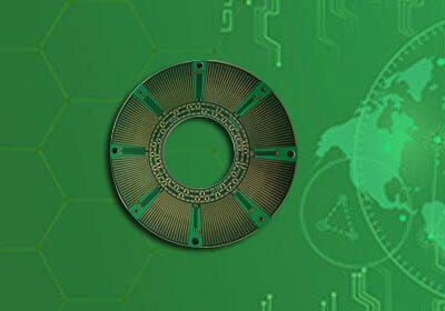

Model : 44layers IC Probe Card PCB
Material : TUC/TU872HF
Layer : 44Layers
Color : Green
Size: 20 "* 22"
Structure: L1-L44 10mil
L1-L28 12mil
L29-L44 14mil
Surface technology: hard gold 3-15u
Special process: metal cladding, depth control drilling
Application : IC(Integrated Circuit Chip) test PCB
1. Probe card is the interface between chip under test and testing machine in wafer test. It is mainly used to measure the electrical performance of chip before chip packaging, and to screen out the bad chip before packaging.
2. Integrated circuit (abbreviated as IC) is a kind of integrated electronic circuit, which uses semiconductor manufacturing technology to make many transistors, resistors, capacitors and other components on a small silicon chip, and combines the components into a complete electronic circuit according to the multi-layer wiring method
3. Probe cards are divided into blade card, cantilever card, vertical card, membrane card and MEMS card
4. The probe card is mainly composed of PCB, probe and functional components. According to different situations, there will be demands for electronic components and stiffener. The cantilever card also includes ring, epoxy, etc
5. The common materials of cantilever pin clip are tungsten tungsten (W), rhenium tungsten (RW, 3% R, 97% w), beryllium copper (BeCu), paliney7 (P)
6. PCB is the carrier of the needle, ring and functional parts, and realizes the signal transmission between the needle tip and the testing machine. Its shape and size are restricted by the interface mode, and the material is restricted by the testing environment. The corresponding shapes are generally square and round

7. MEMS: in order to improve throughput and develop probe card technology with fine pitch and high pin counts, micro electrical mechanical systems; The emergence of MEMS technology breaks through the technical limitations of manual assembly of epoxy ring probe card and welding of micro spring probe card one by one. It has a high degree of automation and breaks through the limitation that the production cost is proportional to the number of pin counts, which is conducive to the production of high pin count probe card, It is suitable for high pin count (~ 30K pins / card), high current and high probe compression stroke. Excellent stability and low test scratch. In other words, in the wafer test of very narrow spacing, only minimal scratch marks are produced, which can effectively increase the durability and reduce the frequency of needle changing.
8. The number of stuck needles of epoxy cantilever probe can reach thousands, and the number of needle layers can reach 16; Pitch cantilever needle 30um, vertical needle 40-50um
9. Service life of cantilever probe card: 100wtd
10. Storage conditions of probe card: vacuum packaging, leaving factory, idle probe card stored in nitrogen gas holder, humidity: 25% ± 2
Model : 44layers IC Probe Card PCB
Material : TUC/TU872HF
Layer : 44Layers
Color : Green
Size: 20 "* 22"
Structure: L1-L44 10mil
L1-L28 12mil
L29-L44 14mil
Surface technology: hard gold 3-15u
Special process: metal cladding, depth control drilling
Application : IC(Integrated Circuit Chip) test PCB
For PCB technical problems, iPCB knowledgeable support team is here to help you with every step. You can also request PCB quotation here. Please contact E-mail sales@ipcb.com
We will respond very quickly.


