

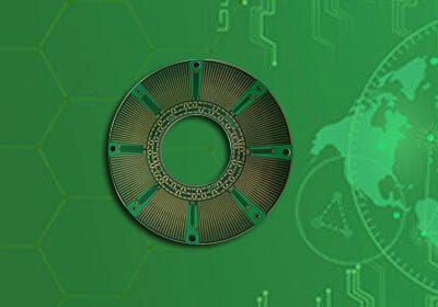

Model : Burn-in Board
Material : High TG TG175
Layer : 20Layers
Color : Green
Size : 610 * 572mm
Board Thickness: 3.2mm
BGA number: 24
Surface technology: Immersion Gold(3U)
Copper thickness: inner layer 70/35um, outer layer 35um
Application : IC burn-in test board (BIB) PCB
The IC burn in board (BIB) is used as a carrier for semiconductor ICs. The IC to be tested is connected to the IC burn-in test board BIB (Burn-In Board) through SOCKET or other methods, and placed in the test machine to the different temperatures of the IC, Voltage, signal, etc. to test the reliability of the IC.

BIB (Burn-In Board) burn in board products:
(1) HTOL test (High-temperature Operation Life)
HTOL is mainly to simulate the life test of IC in high temperature environment, continuous power (voltage or current), to detect whether the functionality and characteristics of the IC itself will change due to environmental conditions, and to evaluate the long-term operation of the IC life.
(2) HAST test (High Accelerated Stress Test)
It is simulated that when the IC is exposed to extremely high temperature and humidity, the accelerated water vapor will penetrate into the interior through the interface between the external protective material and the metal wire to evaluate the resistance of the IC structure to moisture.
IPCB is a BIB (Burn-In Board) burn-in test board manufacturer, providing professional BIB (Burn-In Board) burn-in test board manufacturing.

Several requirements of BIB (Burn-In Board) burn in board:
1. In order to prevent chip power or signal short circuit from causing other chips to fail to work, each chip power supply needs to be independent and connected to the main power supply through a resistor.
2. When the current of the trace is greater than 500mA, it needs to be marked in the schematic diagram.
3. If the high-frequency wiring has impedance matching, the copper foil thickness, line width and PCB board material should be given.
4. Sensitive ports, devices, etc. that need to be shielded or other special treatments need to be clearly marked.
5. The crystal oscillator circuit needs to give a typical application circuit, including the matching capacitance value.
6. It is necessary to specify whether the analog circuit and the digital circuit and the paving need to be divided or divided.
7. If you need to provide an external signal source, give the driving capability and related indicators of the required signal source.
8. PCB board has no abnormal deformation or distortion under high temperature (150 degree Celsius) for a long time.
9. PCB circuit will not have any short circuit or open circuit due to high temperature environment.
Model : Burn-in Board
Material : High TG TG175
Layer : 20Layers
Color : Green
Size : 610 * 572mm
Board Thickness: 3.2mm
BGA number: 24
Surface technology: Immersion Gold(3U)
Copper thickness: inner layer 70/35um, outer layer 35um
Application : IC burn-in test board (BIB) PCB
For PCB technical problems, iPCB knowledgeable support team is here to help you with every step. You can also request PCB quotation here. Please contact E-mail sales@ipcb.com
We will respond very quickly.


