A PCB circuit board design mainly includes the steps of clarifying product requirements, PCB hardware system design, device selection, PCB drawing, PCB production proofing, welding and debugging. So what are the points to pay attention to in these steps? The editor will take you to the fine product, you must fine product!
1. Clear needs
At the beginning of a hardware PCB design, the first thing to do is to clarify the requirements of the product, which mainly includes clarifying the functional requirements and appearance. The main functions need to be clarified, and a small amount of additional functions can be added later, but the main functions of the product should not be affected. The determination of the product shape is very important, which will affect the later PCB drawing and component selection.
2. Hardware system design
In hardware system design, the power supply mode, sensor type, communication mode, human-computer interaction mode, reserved interface, etc. of the product should be determined according to the functional requirements of the product. Generally, you can use Visio to draw the block diagram of the system. The block diagram of the system should be able to describe the relationship between the various module circuits of the hardware system, and the module components of the entire system.
3, device selection
In the device selection stage, you need to select related devices according to your own product functions, which generally include the selection of chips such as power supply, main control, sensors, communications, and storage. The selection needs to consider the function, price, supply and other factors of the chip to choose a suitable chip for your product. Chip selection channels can be compared through large-scale chip electronic component malls such as Lichuang Mall, Yunhanxincheng, and Dejie Electronics.

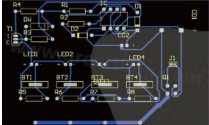
4, PCB drawing
PCB drawing involves the EDA software of PCB design. At present, the mainstream PCB design tool software used by engineers and technicians engaged in circuit design in China are Allegro, PADS and Altium Designer. Beginners recommend using Altium Designer, there will be more tutorials online.
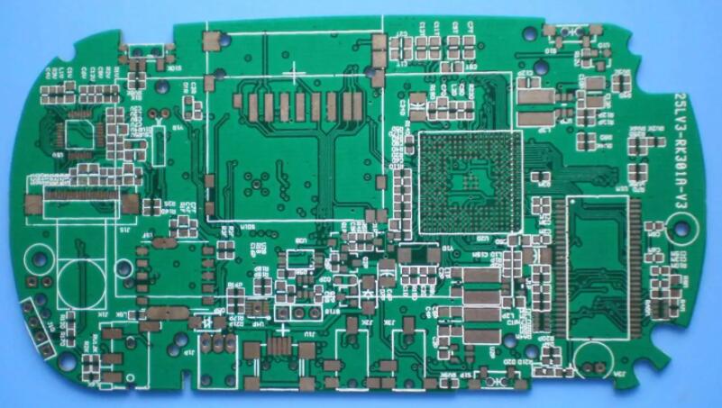
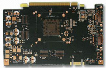
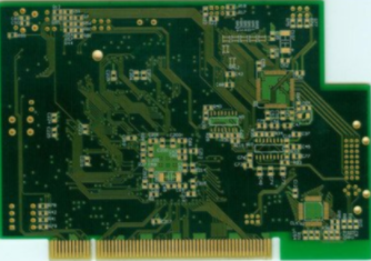
5, PCB production proofing
After the PCB is designed, you can go to the PCB manufacturer for proofing. Before production, you need to provide the manufacturer with production documents. One is to directly provide the PCB file. This method will risk the product being leaked. Then the safer is to provide the gerber file. The proofing price of the sample is generally between 50-100 yuan, and the delivery time is generally 24 hours. Of course, special PCBs will be different. It is recommended to go to PCB, Jiali Chuang, Jiefang and other large manufacturers for proofing, to avoid PCB production problems that may cause abnormal debugging later. This situation will make you suspicious of life later in debugging.
6, welding test
After the PCB and components are in place, you can solder. The necessary tools for soldering: soldering iron and air gun. As for the tweezers, it depends on the technology. Welding is generally divided into direct manual welding and brushed steel mesh welding. Direct welding tests the craftsmanship, and the welding is not good-looking. If you brush the stencil welding, you can place the stencil order together when you produce the PCB. Generally, a stencil is 50. After using the stencil to brush the solder paste, if possible, put it on the machine, if not, put it in the hand. It can be baked in a reflow oven, or it can be blown with an air gun.