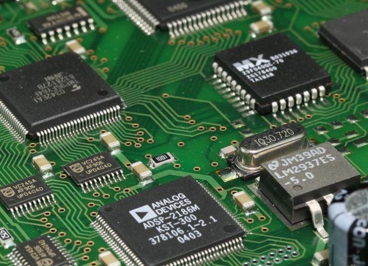
Copper foil (copper foil): a kind of cationic electrolytic material, a thin, continuous metal foil deposited on the base layer of the circuit board, which acts as the conductor of the PCB. It is easy to adhere to the insulating layer, accept the printed protective layer, and form a circuit pattern after corrosion. The following editor will talk about the thickness of the copper foil for PCB proofing and how to choose the appropriate copper thickness for PCB proofing.
Commonly used international PCB copper thicknesses are: 17.5um, 35um, 50um, 70um. The thickness of the PCB proofing copper foil is produced according to the requirements of the customer when placing the order. If there is no special description, the single and double panels are generally 1A copper, which is 35um.
But sometimes the current is relatively large, the product is relatively special circuit board, will use 3OZ, 4OZ, 5OZ...8OZ, Shenzhen Chengxuan circuit can currently achieve 8A copper, which is 280um, if there is a need for thick copper You can contact me.
Generally, the thickness of copper foil (copper) of single and double-sided PCB boards is about 35um (1.4mil), and the other specifications are 50um and 70um. The thickness of the surface layer of the multilayer board is generally 35um=1oz (1.4mil), and the inner layer is 17.5um (0.7mil). 70% of the circuit boards use 35um copper foil thickness, which mainly depends on the use of the PCB and the size of the signal voltage and current; in addition, for PCBs that require excessive current, some will use 70um copper thickness and 105um copper thickness, There will rarely be 140um and so on.
The thickness of the copper skin is usually expressed in oz (ounces). 1oz refers to the thickness of the copper that 1oz of copper evenly covers an area of 1 square foot, which is about 1.4mil. It is the weight per unit area to express the average thickness of the copper foil . Expressed by the formula, 1oz=28.35g/FT2 (FT2 is square feet, 1 square foot=0.09290304 square meters).
For different purposes, the thickness of the copper skin is also different, the ordinary 0.5oz, 1oz, 2oz, mostly used in consumer and communication products. Thick copper products above 3oz are mostly used for high current, such as high voltage products, power boards!
The thickness of the copper skin (the width of the trace) will affect the current. Although there are formulas that can directly calculate the maximum current carrying capacity of the copper foil, it is not so simple in the actual design of the circuit. Therefore, the safety should be fully considered in the design. Factors are taken into consideration.
The above is what the editor introduced about the thickness of the copper foil for PCB proofing and how to choose the appropriate copper thickness for PCB proofing. I hope it will be helpful to everyone. If you have any questions, please contact QQ, WeChat or phone on the right., We will have professional staff to answer you.
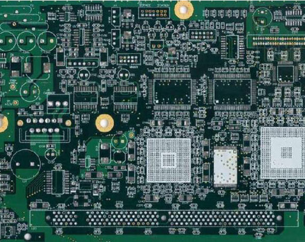
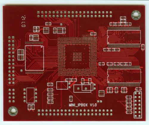
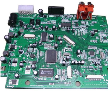
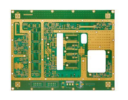
PCB (Printed Circuit Board), the Chinese name is printed circuit board, also known as printed circuit board, is an important electronic component, a support for electronic components, and a carrier for electrical connection of electronic components. Because it is made by electronic printing, it is called a "printed" circuit board.
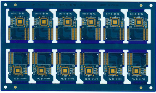
With the continuous upgrading of electronic products, new products that meet the needs of users continue to appear in the market. These products need to undergo continuous proofing and testing before they go on the market in order to meet the needs of more users.
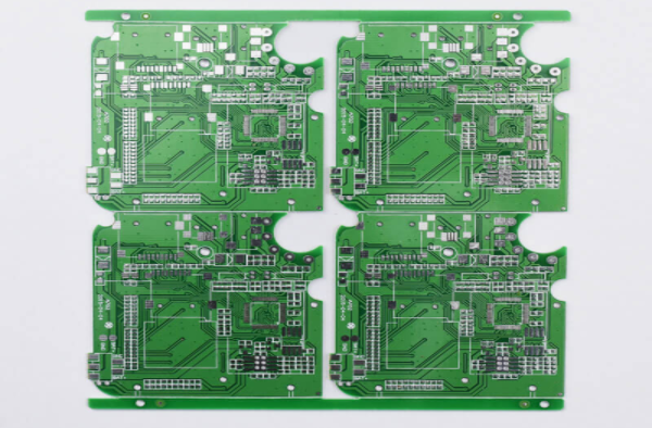
Circuit board proofing generally means that after the engineer's PCB layout design is completed, the electronic product is sent to the PCB manufacturer to be processed into a circuit board for trial production. Because it is a newly developed product, many functions are not yet complete, and there are many functions that need to be debugged. Mass production can only be carried out after the debugging is qualified. If the debugging is unqualified, it needs to be revised, proofed and debugged, which will reduce a lot of unnecessary in the later stage. Trouble.
1. For manufacturers, the matters needing attention are:
1. Carefully check the relevant PCB documents to avoid data problems;
2. Complete process approval and configuration with its own process;
3. In-depth communication with customers, detailed understanding of customer requirements and precautions, to prevent mistakes.
2. For engineers, the matters needing attention are:
1. It is necessary to select a reasonable quantity of proofing according to different situations to reduce costs;
2. Specially confirm the device packaging to avoid proofing failure due to packaging errors;
3. Fully inspect the PCB to improve performance;
4. Do a good job in signal integrity layout to reduce noise and improve stability.

4, the PCB proofing process, the matters needing attention are as follows:
1. Layout and routing of components
The layout and wiring of the components have a great impact on the life, stability, and electromagnetic compatibility of the product, so special attention should be paid. Need to pay attention to the placement order of the components, usually first place the components in a fixed position related to the structure, and place other components from the largest to the smallest. In addition, the component layout needs to pay attention to the heat dissipation problem. The heating components should be distributed and not concentrated in one place.
2. Adjust and perfect
After the PCB wiring is completed, some adjustments to the text, individual components, and wiring and copper plating are required for production, debugging, and maintenance.
3. Use simulation function for PCB proofing
In order to ensure that the PCB can be proofed correctly, software can be used for simulation. Especially for high-frequency digital circuits, some problems can be found in advance and the workload of later debugging can be reduced.
The above is what the editor introduces about PCB proofing and what matters need to be paid attention to. I hope it will be helpful to everyone. If you still have any questions, please contact QQ, WeChat or phone on the right, we will have a professional The staff will answer for you.
With the continuous development of the electronics industry, the products are not updated, leading to the upstream supplier of electronic products, the circuit board industry is becoming more and more busy. Due to the increasingly fierce market competition, the price issue has become a problem that buyers are more concerned about. I will talk about the price of PCB proofing and the price of PCB proofing in detail, which is more affordable. I hope it can help everyone.
Circuit board proofing generally means that after the engineer completes the PCB layout design, the electronic product is sent to the circuit board manufacturer to be processed into a circuit board for testing. Because it is a newly developed product, many functions are not yet complete, and there are many functions that need to be debugged. Mass production can only be carried out after the debugging is qualified. If the debugging is unqualified, it needs to be revised, proofed and debugged, which will reduce a lot of unnecessary in the later stage. Trouble.
With the increasingly fierce market competition, the price issue has become a concern for buyers. The characteristic of PCB proofing price is that it changes with the quantity of proofing and the delivery time of proofing. Generally speaking, it is an ordinary single and double. Panel, no rush, the quantity is less than 10 pieces, conventional craftsmanship, the size is within 100*100mm, generally only 50 yuan, but if your quantity is more than this, the delivery time will have to be expedited, and the price will be different. The price should be calculated according to the data, quantity and delivery date.
If it is an ordinary four-layer, no rush, the quantity is less than 10 pieces, the conventional technology, the size is within 100*100mm, generally only 200 yuan, the price also changes with the quantity, the difficulty of the data, and the change in delivery time. . In this case, it is best to consult customer service.