Six things to consider when transferring PCB schematics to layout design. All the examples mentioned are developed using the Multisim design environment, but the same concepts apply when using different EDA tools!

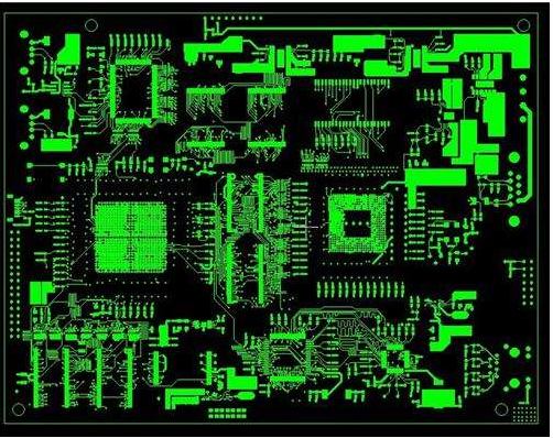
Initial schematic transfer
In the process of transferring the schematic to the layout environment through the netlist file, device information, netlist, layout information and initial trace width settings will also be transferred.
Here are some recommended steps to prepare for the layout design phase:
1. Set the grid and unit to appropriate values. In order to achieve more precise layout control of components and traces, the device grid, copper grid, via grid and SMD grid can be designed to be 1mil.
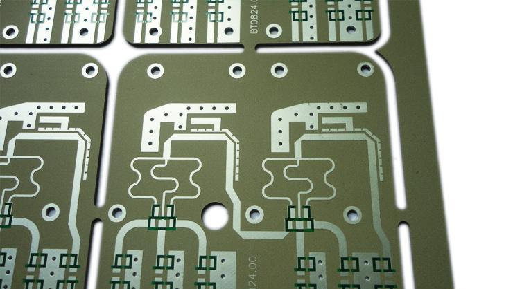
2. Set the blank area and vias of the outer frame of the circuit board to the required values. PCB manufacturersmay have specific minimum or nominal recommended values for blind and buried via settings.
3. Set the corresponding pad/via parameters according to the ability of the PCB manufacturer. Most PCB manufacturers can support smaller vias with a bore diameter of 10 mils and a pad diameter of 20 mils.
4. Set design rules according to requirements.
5. Set custom shortcut keys for commonly used layers, so that you can quickly switch layers (and create vias) during routing.
Handling errors in the transfer process of schematic diagrams
A common error in the schematic transfer process is non-existent or incorrect package assignment. have to be aware of is:
If there is a device in the schematic diagram that is not packaged, a warning message will pop up, indicating that the virtual component cannot be exported. In this case, no default packaging information will be passed to the layout, and the components will simply be deleted from the layout.
If the package transfer has passed, but the effective package shape cannot be correctly matched, an alarm message indicating the mismatch will also be generated during the transfer process.
Correct the package assignment in the schematic or create a valid package for any device. After correction, perform the forward labeling step to update and synchronize the design information.
Update the design with annotations
Annotation is the process of transferring design changes from the schematic to the layout or from the layout to the schematic. Backward labeling (from layout to schematic) and forward labeling (from schematic to layout) are the keys to keeping the design accurate.
In order to protect the work that has been done, the current version of the schematic and layout files need to be backed up and archived before any important forward or backward annotation steps.
Don't try to make changes in the schematic and layout at the same time. Make changes to only one part of the design (either the schematic or the layout), and then perform the correct annotation steps to synchronize the design data.
Renumber the device
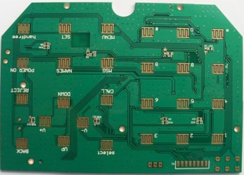
Device renumbering refers to a function of renumbering the components on the PCB in a specific order. The reference numbers should be sorted from top to bottom and from left to right on the PCB. This makes it easier to locate the device location on the board during assembly, testing, and troubleshooting.
Handle last-minute device or netlist changes
Last-minute PCB device or netlist changes are not desirable, but sometimes they have to be done because of device availability issues or detection of last-minute design errors. If you need to change the component or netlist, it should be done in the schematic, and then forward annotated to the layout tool. Here are some tips:
1. If a new device is added after the layout design starts (for example, a pull-up resistor is added to the open-drain output), then resistors and networks are added to the design from the schematic diagram. After being marked in the forward direction, the resistor will be displayed outside the circuit board frame as an un-layout component, and a flying line will be displayed to indicate the connection to the network. Next, move the components to the outer frame of the circuit board and perform normal wiring.
2. Backward labeling and reference label changes can work well together, such as renumbering the rear layout.
Select the positioning device by highlighting
In the PCB layout process, one way to browse specific components or traces in the schematic is to use the ‘highlight selection’ function. This function allows you to select a component or a trace (or multiple objects), and then view their position in the schematic.
This function is especially useful when matching bypass capacitors and their corresponding IC connections. Conversely, you can also locate specific components or traces in the layout when browsing the schematic.