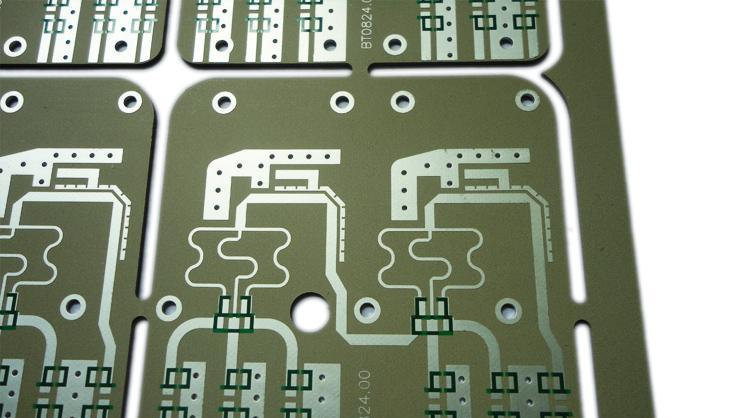
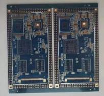
Copper coating is to use the unused space on the PCB circuit board as a reference surface, and then fill it with solid copper. These copper areas are also called copper filling.
The significance of copper coating is to reduce the impedance of the ground wire and improve the anti-interference ability; reduce the voltage drop and improve the efficiency of the power supply; connecting with the ground wire can also reduce the loop area. Also for the purpose of making the PCB as not deformed as possible when soldering, most PCB manufacturers will also require PCB designers to fill the open area of the PCB with copper or grid-like ground wires. If the copper is not handled properly, it will Whether the gains or losses are rewarded or lost, is the copper coating "the advantages outweigh the disadvantages" or "the disadvantages outweigh the advantages"?

Everyone knows that under high frequency conditions, the distributed capacitance of the wiring on the printed circuit board will work. When the length is greater than 1/20 of the corresponding wavelength of the noise frequency, an antenna effect will occur, and the noise will be emitted through the wiring. If there is a poorly grounded copper pour in the PCB circuit board, the copper pour becomes a tool for noise transmission. Therefore, in a high-frequency circuit, do not think that the ground wire is connected to the ground. This is "Ground wire", must be less than λ/20, punch holes in the wiring, and "good ground" with the ground plane of the multilayer board. If the copper coating is handled properly, the copper coating not only increases the current, but also plays a dual role of shielding interference.
There are generally two basic methods for copper coating, namely large-area copper coating and grid copper. It is often asked whether large-area copper coating is better than grid copper coating. It is not good to generalize. Why? Large-area copper coating has the dual functions of increasing current and shielding. However, if large-area copper coating is used for wave soldering, the board may lift up and even blisters. Therefore, for large-area copper coating, several grooves are generally used to alleviate the blistering of the copper foil. The pure mesh copper coating is mainly used for shielding, and the effect of increasing the current is reduced. From the perspective of heat dissipation, the mesh is beneficial (It lowers the heating surface of the copper) and plays a role of electromagnetic shielding to a certain extent.
However, it should be pointed out that the grid is made up of traces in staggered directions. We know that for the circuit, the width of the trace has a corresponding "electrical length" (actual size) for the operating frequency of the circuit board. Divide by the digital frequency corresponding to the working frequency, see related books for details). When the working frequency is not very high, perhaps the role of the grid lines is not very obvious. Once the electrical length matches the working frequency, it will be very bad. You will find that the circuit does not work properly at all, and signals that interfere with the operation of the system are being emitted everywhere.
Therefore, for colleagues who use grids, my suggestion is to choose according to the working conditions of the designed circuit board, and don't cling to one thing. Therefore, high-frequency circuits have high requirements for multi-purpose grids for anti-interference, and low-frequency circuits have circuits with large currents, such as commonly used complete copper.
Then we need to pay attention to what issues in copper pour in order to achieve the desired effect of copper pour:
1. For single-point connections to different grounds, the method is to connect through 0 ohm resistors or magnetic beads or inductance.
2. Pour copper near the crystal oscillator. The crystal oscillator in the circuit is a high-frequency emission source. The method is to pour copper around the crystal oscillator, and then ground the shell of the crystal oscillator separately.
3. The island (dead zone) problem, if you think it is too big, it won't cost much to define a ground via and add it in.
4. At the beginning of wiring, the ground wire should be treated the same. When routing the ground wire, the ground wire should be routed well. You cannot rely on adding vias to eliminate the ground pins for the connection after copper plating. This effect is very bad.
5. It is best not to have sharp corners on the board (less than or equal to 180 degrees), because from the perspective of electromagnetics, this constitutes a transmitting antenna! There will always be an impact on others, but it is big or small That's it, I recommend using the edge of the arc.
6. If the PCB circuit board has more grounds, such as SGND, AGND, GND, etc., according to the position of the PCB board, the main "ground" is used as a reference to independently pour copper, digital ground and It is not much to say that the copper pour is separated by analogy. At the same time, before the copper pour, first thicken the corresponding power connection: 5.0V, 3.3V, etc., in this way, multiple deformed structures of different shapes are formed.
7. Do not pour copper in the open area of the middle layer of the multilayer board. Because it is difficult for you to make this copper clad "good ground".
8. The metal inside the equipment, such as metal radiators, metal reinforcement strips, etc., must be "good grounding".
9. The heat dissipation metal block of the three-terminal regulator must be well grounded. The ground isolation strip near the crystal oscillator must be well grounded. If the grounding problem is dealt with for the copper coating on the PCB circuit board, it is definitely "pros outweigh the disadvantages". It can reduce the return area of the signal line and reduce the electromagnetic interference of the signal to the outside.