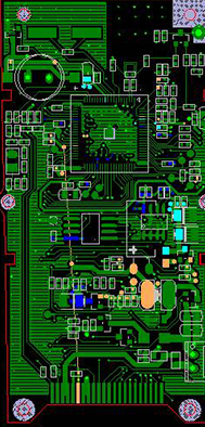
Many characteristic impedance modules can finally be divided into two modes: microstrip line and strip line. Among them, the surface of the microstrip line is coated with a single-ended structure, such as electroplating and etching. The production of a characteristic impedance board is successful or not, the wire width plays a decisive role
Many characteristic impedance modules can finally be divided into two modes: microstrip line and strip line. Among them, the surface of the microstrip line is coated with a single-ended structure, such as electroplating and etching. Whether the production of a characteristic impedance board is successful or not, the wire width plays a decisive role. It requires the PCB board manufacturer to consider an appropriate compensation amount from the time of making the engineering documents. Of course, this compensation amount is obtained through the manufacturer's experiment. At the same time, the etching speed and other related parameters need to be considered during the etching after electroplating, and the first board test and the AOI or slicing test need to be performed. When setting the width of the impedance line, the PCB designer must know the processing ability of the PCB manufacturer in advance. This is also the standard for examining whether the PCB manufacturer is a qualified characteristic impedance board manufacturer.
Regarding the above production parameters, if the PCB designer does not go to the manufacturer to understand, but asks the manufacturer to improve their production parameters based on the theoretical data of the design, it is relatively unlikely, because the PCB manufacturer is not only targeting you When creating impedance models, the general PCB designers tend to ignore the surface coating. Si8000 can simulate the surface circuit and the solder mask thickness on the substrate to calculate a more reasonable impedance value. Because solder mask can affect the final characteristic impedance value of 1 to 3 ohms, this must be considered for characteristic impedance boards with smaller and smaller error requirements. In addition, the new Si8000 software can also calculate the odd-mode impedance, even-mode impedance, and common-mode impedance in the differential impedance. In high-speed systems such as USB2.0 and LVDS, it is increasingly necessary to control these characteristic impedances.

In addition, the Si8000 also uses a multi-unit input method, allowing you to directly input data without conversion. Currently, 4 types of input units are provided: mils, inches, micrometers, and millimeters. Because the characteristic impedance is generally allowed to have a tolerance of ±10%, and there will be certain errors in each parameter in production, the Si8000 can calculate the limit value at the same time when calculating the impedance (Figure 9), which greatly provides convenience for production. In addition, the Si8000 can inversely infer relevant parameters based on the impedance value, which is very useful for PCB designers and manufacturers and can save more time.
In addition, due to side corrosion in production, the upper and lower ends of the finished board wires will be unequal. Therefore, it is necessary to confirm the difference between the upper and lower ends of the wire with the PCB manufacturer, so as to simulate the impedance value closer to reality through software.
(1) Media thickness: The impedance is proportional to it. The thickness of the medium is mainly obtained by measuring the actual medium after the laminate in production is laminated. Therefore, when the PCB designer considers the thickness of the medium, it is necessary to know the thickness of the commonly used inner core board and the semi-cured (PP) sheet of the PCB manufacturer and the thickness after lamination (and also need to understand
Sheet cost and simplification of production), this thickness is not only related to the inner core board and prepreg (PP) sheet, but also related to the pattern distribution of the upper and lower lines. The same prepreg (PP) sheet is pressed between two large copper surfaces. The thickness of the joint after pressing between the two lines is not equal. When calculating the characteristic impedance, it is also necessary to consider whether this thickness contains the thickness of the copper foil. Generally, the thickness of the inner core board with two decimal places does not contain copper foil, that is, the thickness of the inner core board with two decimal places is the thickness of the medium + the thickness of two layers of copper foil.
(2) Wire spacing: Wire spacing is closely related to wire width and thickness, and its main influencing factors are the same as the previous analysis of wire width and thickness. Determined by the board and the production process, the PCB designer also needs to know from the manufacturer.
(3) Solder mask thickness: impedance is inversely proportional to it. For characteristic impedance boards, some do not require printed solder resist, such as antenna microstrip boards, but some boards require printed resist solder. Printed board before and after screen printing
The impedance value is different, so this is also a parameter that needs to be considered, and it needs to be understood from the PCB manufacturer, and the thickness of the solder mask printed on the line and the solder mask printed on the substrate is different.
Among the three main parameters mentioned above, the dielectric thickness has the greatest impact, followed by the dielectric constant and line width, and finally the copper thickness. The least impact is the solder mask thickness.