Super difficult Four-sided carbon fiber body This will be a very difficult process. First of all, let's listen to what kind of ideas the Azumino factory of VAIO headquarters has to manufacture products. Shimizu: Our goal is to produce products that can be trusted by customers. VAIO has always attached great importance to the trust relationship with customers. This relationship is measured by the manufacturer through sensory testing (using human vision, touch and other senses. Detection) or manual assembly. In addition, we also design and ensure stable production of small equipment (a general term for components that can support the processing and assembly of components) and large equipment such as presses. Our main advantage is to ensure stable work quality, ultra-high precision and various We believe that using the respective strengths of humans, machines and equipment to improve production quality is closely related to winning the trust of customers.

Chip packaging
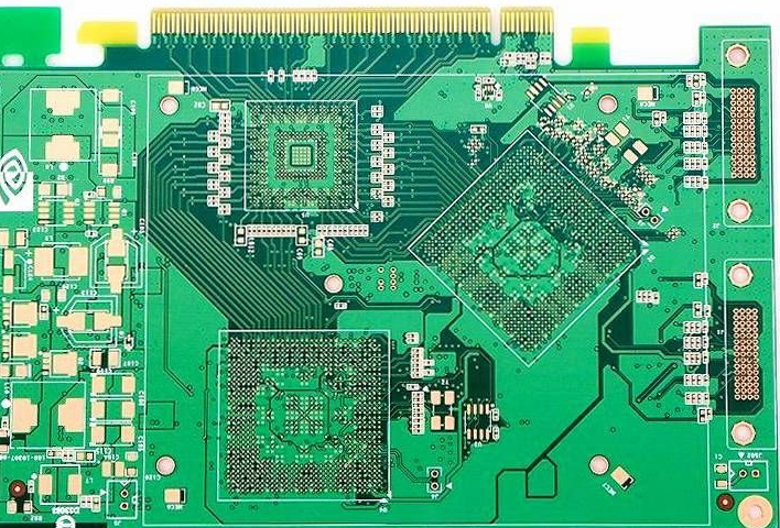
BGA (ballgridarray) BGA package physical [1] ball contact array, one of the surface mount packages. On the back of the printed circuit board, spherical bumps are produced in the display mode to replace the pins, and the LSI chip is assembled on the front side of the printed circuit board, and then sealed by molding resin or potting. Also known as bump display carrier (PAC). The pin can exceed 200, which is a package for multi-pin LSI. The package body can also be made smaller than QFP (Quad Flat Package). For example, a 360-pin BGA with a pin center distance of 1.5mm is only 31mm square; while a 304-pin QFP with a pin center distance of 0.5mm is 40mm square. And BGA does not have to worry about pin deformation like QFP.
Layout line width and spacing traces teardrop vias [6 details to quickly improve the quality of PCB boards]
Preface Now many PCBLayou t engineers complete the layout and routing according to the constraint rules given by hardware engineers or PISI engineers, commonly known as "wire pullers". If you don't want to be treated as a "wire puller". Have a certain circuit understanding and the ability to do PI/SI analysis with SI/PI engineers.PCBLayout is a technical job, but also an experience job. Learning some useful experience can often benefit people a lot. PCB layout structure Layout, literally explained, is the reasonable placement of circuit components.