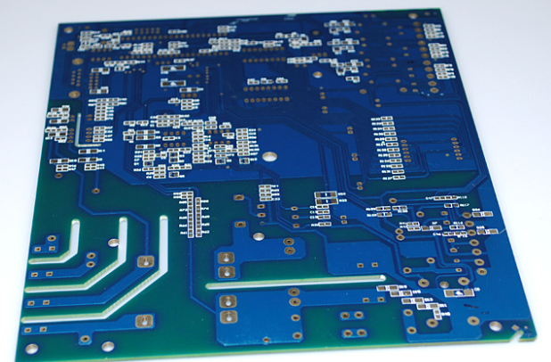
What issues should be paid attention to when designing high-speed PCB vias?
PCB vias are mainly composed of three parts: the hole, the pad area around the hole, and the POWER layer isolation area. In high-speed PCB design, multi-layer PCBs are often used, and vias are an important factor in multi-layer PCB design. In the high-speed PCB multilayer board, the signal transmission from one layer of interconnection line to another layer of interconnection line needs to be connected through vias. So, what issues should be paid attention to when designing high-speed PCB vias?
High-speed PCB via design
1. Choose a reasonable via size. For multi-layer general-density PCB design, the ideal via sizes for drilling, pads, and POWER isolation areas are 0.25mm, 0.51mm, and 0.91mm; for some high-density PCBs, 0.20 can also be used. mm, 0.46mm, 0.86mm vias, you can also try non-through vias; for power or ground vias, you can consider using a larger size to reduce impedance.
2. The larger the POWER isolation area, the better.

3. Try not to change the layers of the signal traces on the PCB, that is, minimize vias.
4. Using a thinner PCB is beneficial to reduce the two parasitic parameters of vias.
5. The power and ground pins should be close to the vias, the shorter the lead between the vias and the pins, the better; at the same time, the power and ground leads should be as thick as possible to reduce impedance;
6. Place some grounding vias near the vias of the signal change layer to provide a short-distance loop for the signal.
7. The length of the via is also the main factor affecting the inductance of the via. In high-speed PCB design, in order to reduce the problems caused by vias, the length of vias is generally controlled within 2.0mm. For vias with a length greater than 2.0 mm, the continuity of via impedance can be improved to a certain extent by increasing the aperture of the via. When the via length is 1.0 mm or less, the best via hole diameter is 0.20 mm ~ 0.30 mm.
The above are the issues that need attention in high-speed PCB via design. Have you mastered it? ipcb is a high-precision, high-quality PCB manufacturer, such as: isola 370hr PCB, high-frequency PCB, high-speed PCB, ic substrate, ic test board, impedance PCB, HDI PCB, Rigid-Flex PCB, buried blind PCB, advanced PCB, microwave PCB, telfon PCB and other ipcb are good at PCB manufacturing.