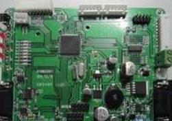
Basic knowledge of PCB pad design?
In the layout of PCB components, designers should consider the difference between the minimum spacing between components relative to the thickness of the components. Normally, the spacing between larger electronic components should be increased to avoid the addition of thin components and ultimately cause Welding defects. Secondly, the components are fixed on the PCB by soldering through the lead holes on the PCB, and the printed wires connect the pads to realize the electrical connection of the components in the circuit. In the process of soldering, if people who do not understand this aspect, it is easy to damage the pads on the PCB, which will seriously cause the entire circuit board to be scrapped. The following editor will tell you some basic common sense about pads.
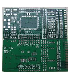
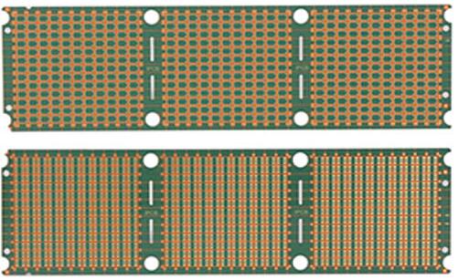
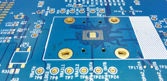
As mentioned earlier, the component is fixed on the PCB by soldering through the lead hole on the PCB, then the lead hole and the surrounding copper foil are called the pad, which is the basic unit of surface mount assembly to form the circuit The land pattern of the board, that is, various land combinations designed for special component types.

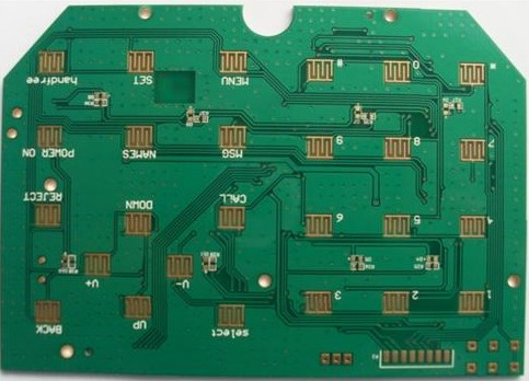
Our common pad shapes are square pads, which are often used when the printed circuit board components are large and few, and the printed wires are simple. It is easy to use this kind of pads when making a PCB by hand. There is also a circular pad: widely used in single and double-sided printed boards with regularly arranged components. If the density of the board allows, the pad can be larger so that it will not fall off during soldering.
The size design of PCB pads also has corresponding standards, that is, the minimum single side of all pads is not less than 0.25mm, and the maximum diameter of the entire pad is not more than 3 times the component aperture. In the case of dense wiring, it is recommended to use oval and oblong connection plates. The diameter or minimum width of the single-sided board pad is 1.6mm; the weak-current circuit pad of the double-sided board only needs to add 0.5mm to the hole diameter. Too large the pad will easily cause unnecessary continuous soldering. The diameter of the hole exceeds 1.2mm or the diameter of the pad. The pads over 3.0mm should be designed as diamond or quincunx pads. All machine insert parts need to be designed as drip pads along the bent leg direction to ensure full solder joints at the bent leg. The pads on the large-area copper skin should be chrysanthemum-shaped pads, and no virtual soldering.
Special attention is paid to the manual soldering on the PCB, remember not to use a very high temperature soldering iron or tin furnace to operate the pad, because this will easily cause the pad to fall off and cannot be remedied. The above are some of the basic points summarized by the editor. I hope I can help you.
ipcb is a high-precision, high-quality PCB manufacturer, such as: isola 370hr PCB, high-frequency PCB, high-speed PCB, ic substrate, ic test board, impedance PCB, HDI PCB, Rigid-Flex PCB, buried blind PCB, advanced PCB, microwave PCB, telfon PCB and other ipcb are good at PCB manufacturing.