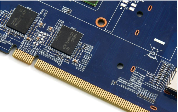
Share about the design and manufacturing of Gold Finger PCB
1. Definition of Golden Finger
The golden finger or edge connector is to insert one end of the PCB board into the connector slot, and connect the connector pin to the outside as the outlet of the PCB, so that the bonding pad or copper sheet contacts the pin at the corresponding position to achieve guidance. For general purposes, and by immersing gold or nickel gold into this PCB pad or copper sheet, this finger like pad is called a gold finger because it is in the shape of a finger.
2. The gold fingers of a PCB can be divided into three types
1) Ordinary gold finger PCB, which is the most common PCB gold finger, has a horizontal or even an array. PCB pads have the same length, width, and space.
2) Uneven gold finger PCB, where the PCB pad width is the same but the length is different, and sometimes the space is also different. For some PCBs, the design purpose of the golden finger is to be shorter than other PCBs. The most relevant example of this type of PCB is a PCB used for memory card readers, where devices connected to long fingers must first supply power to devices connected to shorter fingers.
3) Segmented gold finger PCB, this type of PCB pad has different lengths and the gold finger is segmented. The length of segmented gold fingers varies, and some of them are also disjointed within the same finger on the same PCB. This type of PCB is suitable for waterproof and sturdy electronic products.

Three types of gold finger PCB
3. Surface treatment method for gold finger PCB
Electroplated nickel gold finger PCB: thickness up to 3-50u Due to its excellent conductivity, oxidation resistance, and wear resistance, it is widely used in gold finger PCBs that require frequent insertion and removal or PCBs that require frequent mechanical friction. However, due to the high cost of gold plating, it is only used for gold plating on parts such as gold fingers. PCB factories refer to it as selective gold plating. The color of the gold plating process is silver white, unlike the yellow color of the gold immersion process. The disadvantage is that it can be welded. It is slightly inferior.
Huajin Gold Finger PCB: With a thickness of conventional 1u "and a maximum of 3u", it is widely used in high-precision PCBs with button positions, bonding ICs, BGAs, etc. due to its excellent conductivity, flatness, and solderability. Gold finger PCBs with lower wear resistance requirements can also choose the full board immersion gold process, which is much lower than the cost of the electro gold process. The color of the gold immersion process is golden yellow.

PCB Gold Finger
4. Precautions for Gold Finger PCB Design
When you see shapes and packaging similar to the one shown in the following figure during the PCB design process, your first reaction is that there are gold fingers on the board. A simpler way to determine a golden finger is to have a PIN device on both the top and bottom surfaces of the device, as well as a foolproof U-shaped groove.
When there are gold fingers on the PCB board, it is necessary to handle the details of the gold fingers.
PCB gold finger detail processing includes
1) For PCBs that often require plugging and unplugging, in order to increase the wear resistance of gold fingers, they usually need to be plated with hard gold.
2) To facilitate insertion into the card slot, the gold finger PCB needs to be chamfered, usually at 45 °, with other angles such as 20 °, 30 °, etc. If there are no chamfers in the design, there is a problem. As shown in the following figure, the arrow shows a gold finger PCB design with a 45 ° chamfer:

Golden Finger PCB Chamfer Design
3) The golden finger needs to be used as a whole solder mask to open the window, and the PIN does not need to open the steel mesh.
4) The immersion tin and immersion silver pads need to be at least 14 millimeters away from the top of the fingers, and it is recommended to use a design. When the distance between the pad and the finger position exceeds 1mm, including through hole pads.
5) Do not apply copper to the surface of the golden finger.
6) All layers of the inner layer of the golden finger need to be cut with copper, usually with a width greater than 3mm. You can do half finger cut copper or full finger cut copper. In PCIE design, it is also specified that all copper in the gold finger area should be cut off.
7) The impedance of the golden finger will be relatively low. Cutting copper (knocking down with fingers) can reduce the impedance difference between the gold finger and the impedance line, which is also beneficial for ESD.
8) It is recommended that all copper be cut under a golden finger PCB pad.
Goldfinger PCB play an important role in most electronic products. By understanding each basic aspect of Golden finger PCB, you can confidently choose your best Golden finger PCB manufacturer.