Discussion on RF layout and simple design partition
The meaning of radio frequency
RF circuit board design is often described as a kind of "black art" because there are still many uncertainties in theory. However, RF circuit board design also has many guidelines that can be followed and rules that should not be ignored. But we know that the really practical technique is how to compromise these guidelines and rules when they cannot be implemented accurately due to various design constraints.
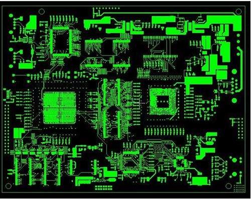
Today's cellular phone design integrates everything together in various ways, which is very detrimental to RF circuit board design. Competition in the industry is fierce now, and everyone is looking for a way to integrate the most functions with the smallest size and the smallest cost. Analog, digital, and RF circuits are tightly packed together, and the space used to separate their problem areas is very small, and considering the cost factor, the number of circuit board layers is often minimized.
RF circuit board design
The design of the RF circuit board is the most troublesome part for design engineers, which requires engineers to plan carefully and pay attention to details.
RF layout concept

When we are in the layout of RF, these principles must be prioritized to be satisfied:
Separate the high-power RF amplifier (HPA) from the low-noise amplifier (LNA) as much as possible, and keep the high-power RF transmitter circuit away from the low-power RF receiver circuit. If there is a lot of physical space on the PCB, this can be done easily, but usually there are many components and the PCB space is small. You can put them on both sides of the PCB, or let them work alternately instead of working at the same time. . High-power circuits sometimes include RF buffers and voltage controlled oscillators (VCO).
Make sure that there is at least a whole piece of ground in the high-power area of the PCB, preferably without vias. Of course, the more copper, the better.
The decoupling of the chip and the power supply is also extremely important, and several ways to implement this principle will be discussed later.
The RF output usually needs to be far away from the RF input, as we will discuss in detail later.
Sensitive analog signals should be as far away as possible from high-speed digital signals and RF signals.
Design partition
The design partition consists of a physical partition and an electrical partition. Physical partitioning mainly involves issues such as component layout, orientation, and shielding; electrical partitioning can continue to be decomposed into partitions for power distribution, RF routing, sensitive circuits and signals, and grounding.
Physical partition
Component layout is the key to achieving a good RF design. The most effective technique is to first fix the components on the RF path and adjust their orientation to minimize the length of the RF path, keep the input away from the output, and as far as possible Ground separation of high-power circuits and low-power circuits.
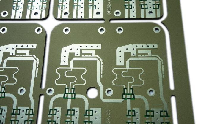
The most effective circuit board stacking method is to arrange the main ground plane (main ground) on the second layer below the surface layer, and route the RF lines on the surface layer as much as possible. Minimizing the size of the vias on the RF path can not only reduce the path inductance, but also reduce the virtual solder joints on the main ground and reduce the chance of RF energy leaking to other areas in the laminate.
In physical space, linear circuits like multi-stage amplifiers are usually sufficient to isolate multiple RF zones from each other, but duplexers, mixers, and intermediate frequency amplifiers/mixers always have multiple RF/IFs. The signals interfere with each other, so care must be taken to minimize this effect. The RF and IF traces should be crossed as much as possible, and a ground should be placed between them as much as possible. The correct RF path is very important to the performance of the entire PCB board, which is why the component layout usually accounts for most of the time in the cellular phone PCB board design.
Despite the above problems, metal shields are very effective and are often the only solution for isolating critical circuits.
In addition, proper and effective chip power decoupling is also very important. Many RF chips with integrated linear circuits are very sensitive to power noise. Usually, each chip needs to use up to four capacitors and an isolation inductor to ensure that all power noise is filtered out.
The minimum capacitance value usually depends on its self-resonant frequency and low pin inductance, and the value of C4 is chosen accordingly. The values of C3 and C2 are relatively large due to their own pin inductance, so the RF decoupling effect is worse, but they are more suitable for filtering lower frequency noise signals. The inductance L1 prevents the RF signal from coupling into the chip from the power line. Remember: all traces are a potential antenna that can both receive and transmit RF signals, and it is also necessary to isolate the induced RF signals from the critical lines.
Remember that inductances are rarely close together in parallel, because this will form an air-core transformer and induce interference signals with each other. The distance between them must be at least the height of one of the devices, or they must be arranged at right angles to reduce their mutual inductance to The smallest.
Electrical partition
The principle of electrical zoning is roughly the same as that of physical zoning, but it also contains some other factors. Some parts of modern cellular phones use different operating voltages and are controlled by software to extend battery life. This means that cellular phones need to run multiple power sources, and this brings more problems to isolation. The power is usually introduced from the connector, and is immediately decoupled to filter out any noise from the outside of the circuit board, and then distributed after passing through a set of switches or regulators.
The DC current of most circuits in cellular phones is quite small, so trace width is usually not a problem. However, a large current line as wide as possible must be routed separately for the power supply of the high-power amplifier to minimize the transmission voltage drop. In order to avoid too much current loss, multiple vias are needed to transfer current from one layer to another. In addition, if it cannot be sufficiently decoupled at the power supply pin of the high-power amplifier, high-power noise will radiate to the entire board and cause various problems. The grounding of high-power amplifiers is critical, and it is often necessary to design a metal shield for it.
In most cases, it is also critical to ensure that the RF output is far away from the RF input. This also applies to amplifiers, buffers and filters. In the worst case, if the output of the amplifier and buffer is fed back to their input with appropriate phase and amplitude, then they may have self-oscillation. In the best case, they will be able to work stably under any temperature and voltage conditions. In fact, they may become unstable and add noise and intermodulation signals to the RF signal.
In short, on each layer of the PCB board, as many grounds as possible should be laid and connected to the main ground. Place the traces as close together as possible to increase the number of plots of the internal signal layer and power distribution layer, and adjust the traces appropriately so that you can arrange the ground connection vias to the isolated plots on the surface. Free ground should be avoided on the various layers of the PCB because they can pick up or inject noise like a small antenna. In most cases, if you can't connect them to the main land, then you'd better remove them.