For PCB drawing board engineers, the most basic process of designing PCB circuit boards can be divided into the following points:
1. The design of the schematic diagram of the PCB circuit board: The design of the schematic diagram of the PCB circuit board is mainly based on the principle diagram design system of PROTEL099 to draw a schematic diagram of the circuit board. In this process, we must make full use of the various schematic drawing tools and various editing functions provided by PROTEL99 to realize our schematic, that is, get a correct, standardized and reasonable circuit schematic.
2. Generate netlist: netlist is a bridge between PCB circuit board schematic design (SCH) and printed PCB circuit board design(PCB). It is the soul of PCB circuit board automation. The netlist can be obtained from the schematic circuit diagram or extracted from the printed PCB circuit board.
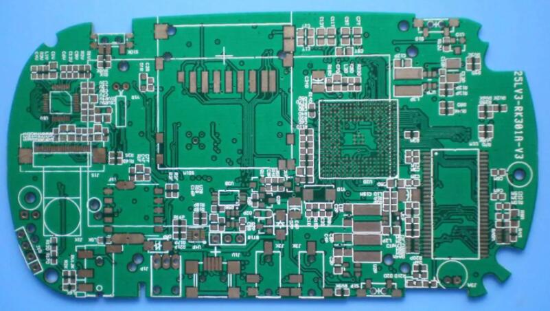
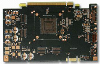
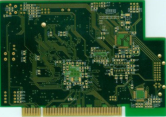
(3) The design of the printed PCB circuit board: The design of the printed PCB circuit board is mainly for another important part of the PCB of PROTEL99. In this process, we use the powerful functions provided by PROTEL99 to realize the PCB circuit board Layout design, complete difficult and other tasks.
But in practice, the specific steps are mainly based on the following subdivision steps:

1. Preliminary work of PCB board design. Use the schematic design tool to draw the schematic diagram and generate the corresponding network table. Of course, in some special cases, such as the PCB circuit board is relatively simple, and there is already a network table, etc., it is not necessary to design the schematic diagram and directly enter the PCB design system. In the PCB design system, you can directly use the parts and packaging. Manually generate the network table. 2. Manually change the network table to define the pads that are not on the schematic diagram of the fixed pins of some components to the network connected to it, and the ground or protective ground without any physical connection can be defined. Change the pin names of some devices with inconsistent pin names in the schematic diagram and PCB package library to be consistent with those in the PCB package library, especially diodes and transistors.
2. Draw the package library of non-standard devices defined by yourself. It is recommended to put all the devices you draw into a special design file for PCB library that you have created.
3. Set the circuit board design environment and draw the printed circuit board frame with a hollow in the middle, etc. 1. The first step after entering the PCB system is to set the PCB design environment, including setting the grid size and type, cursor type, and layout parameters, Wiring parameters and so on. Most of the parameters can use the system default values, and after these parameters are set, they are in line with personal habits and do not need to be modified in the future. 2. Planning the circuit board is mainly to determine the frame of the circuit board, including the size of the circuit board and so on. Put an appropriate size pad on the place where the fixing hole needs to be placed. For 3mm screws, 6.5~8mm outer diameter and 3.2~3.5mm inner diameter pads can be used. For standard boards, it can be imported from other boards or PCBizard. Note-Before drawing the border of the circuit board, the current layer must be set to the shape layer, that is, the wiring layer is prohibited.
4. After opening all the PCB library files to be used, the step of importing the netlist file and modifying the part packaging is a very rigorous step. The netlist is the soul of PCB automatic routing, as well as schematic design and printed PCB circuit board design. Only after the netlist is loaded, can the wiring of the PCB circuit board be carried out. In the process of schematic design, ERC inspection will not involve the packaging of parts. Therefore, when designing the schematic diagram, the packaging of the parts may be forgotten. When the netlist is introduced, the packaging of the parts can be modified or supplemented according to the design situation. Of course, you can manually generate the netlist directly in the PCB, and specify the part package.
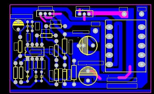
5. Arrange the location of the parts package, also known as the part layout. Protel99 can carry out automatic layout or manual layout. For automatic layout, run "AutoPlace" under "Tools". With this command, you need to have enough patience. The key to routing is layout, and most designers use manual layout. Use the mouse to select a component, hold down the left mouse button, drag the component to the destination, release the left button to fix the component. Protel99 has added some new skills in the layout. New interactive layout options include automatic selection and automatic alignment. Using the automatic selection method can quickly collect similar packaged components, and then rotate, unfold and organize them into groups, and then they can be moved to the desired position on the board. When the simple layout is completed, use automatic alignment to neatly expand or shrink a group of similar components. Tip-In automatic selection, use ShiftX or Y and CtrlX or Y to expand and contract the X and Y directions of the selected component. Note-The layout of parts should be comprehensively considered from the aspects of mechanical structure heat dissipation, electromagnetic interference, and the convenience of future wiring. First arrange the components related to the mechanical size, and lock these components, then the large occupying components and the core components of the circuit, and then the peripheral small components.
6. Make appropriate adjustments according to the situation and then lock all the devices. If the space on the board allows, you can put some wiring areas similar to the experiment board on the board. For large boards, more fixed positioning holes should be added in the middle. Fixed positioning holes should also be added to the side of stressed components such as heavy components or larger plug-ins on the board. If necessary, some test pads can be placed in appropriate positions. It is best to add them in the schematic diagram. Increase the size of the via hole of the pad that is too small, and define the network of all the fixed screw hole pads to the ground or the protective ground. After placing it, use the VIEW3D function to check the actual effect and save it.
Seven, setting the wiring rules is to set the various specifications of the wiring (such as the use level, the line width and spacing of each group, the spacing of the vias, the topological structure of the wiring and other rules, which can be exported from other boards through the Menu of Design-Rules, Import this PCB board again) This step does not have to be set every time, just set it once according to personal habits.