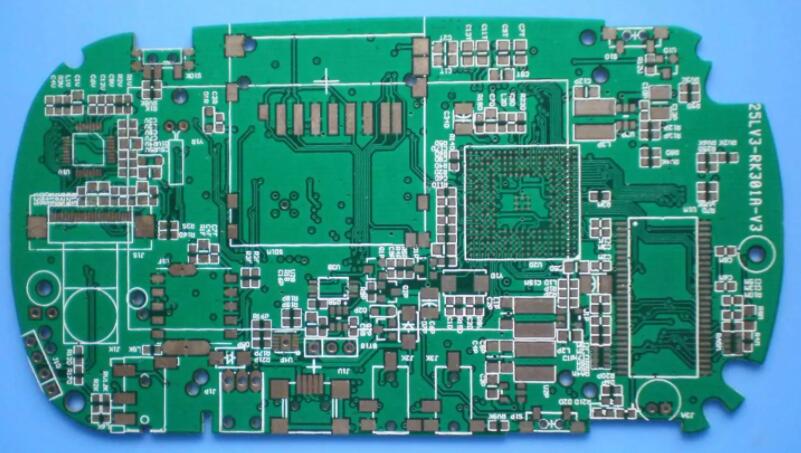
PCB design is indispensable and the most important in the design of electronic products. The quality of PCB design will directly affect the realization of product functions. It is not difficult to design a PCB circuit to realize its function. The difficult thing is that it is not affected by various influences (such as temperature and humidity changes, air pressure changes, mechanical shocks, corrosion, etc.) and can continue to maintain normal and stable work, so we will adopt Various design methods or manufacturing process measures are used to eliminate or reduce these effects to ensure the normal operation of the PCB, such as the use of wider temperature components to adapt to the high temperature or low temperature use environment; try to make the area of the circuit patterns on both sides of the printed board equal To prevent the warpage and deformation of the printed board caused by temperature changes; reasonably arrange the position of large and heavy components on the printed board and design the corresponding installation and fixing structure to prevent the components from falling off due to vibration.
First of all, the most important thing is grounding. Everyone knows that grounding design is the basis of system design. Good grounding is a prerequisite for the safe and stable operation of the system. The broad grounding includes two meanings, namely, grounding and virtual grounding. Ground connection refers to the connection with the earth; connection to the virtual ground refers to the connection with the potential reference point. When the reference point is electrically insulated from the earth, it is called a floating connection. There are two purposes of grounding: one is to ensure the stable and reliable operation of the control system and to prevent interference caused by ground loops, which is often referred to as working grounding; the other is to prevent the operator from being exposed to the risk of electric shock due to the insulation damage or drop of the equipment and guarantee The safety of the equipment is called protective grounding.
If safety grounding is not considered, only from the point of view of the circuit reference point, grounding can be divided into floating ground, single-point grounding, multi-point grounding and mixed grounding. The purpose of floating ground is to isolate the circuit or equipment from the common ground or common wires that may cause circulating currents. The disadvantage of this grounding method is that the equipment is not directly connected to the earth, which is prone to static electricity accumulation, and eventually electrostatic breakdown with a strong discharge current. The usual method is to connect a large resistance between the device and the ground to eliminate the accumulation of static electricity. Single-point grounding means that in a circuit, only one physical point is defined as the ground reference point. Multi-point grounding means that in a system, each grounding point is connected to the ground plane closest to it, so that the length of the grounding lead is the shortest. It is the only practical grounding method for high-frequency signal circuits. Generally speaking, when the frequency is lower than 1MHz, it is better to use single-point grounding; when the frequency is higher than 10MHz, it is better to use multi-point grounding; The length of the ground wire shall not exceed 1/20 of the wavelength, otherwise the multi-point grounding method shall be adopted. Under normal circumstances, in ordinary industrial control systems, the signal frequency is mostly less than 1MHz, so single-point grounding is usually adopted. Hybrid grounding is a combination of single-point grounding and multi-point grounding, and the applicable working frequency range is generally 500kHz~30MHz.
In the computer control system, it is roughly divided into the following types of grounds: analog ground, digital ground, signal ground, system ground, AC ground and protection ground. The analog ground serves as the zero potential of the analog circuits in sensors, transmitters, amplifiers, A-D and D-A converters. The analog signal has accuracy requirements, its signal is relatively small, and it is connected to the production site. Sometimes in order to distinguish the relationship between the weak signal ground of the remote sensor and the analog ground of the host, the ground of the sensor is also called the signal ground. As the zero potential of various digital circuits in computers, digital ground should be separated from analog ground to avoid interference of analog signals by digital pulses. The system ground is the final return point of the above-mentioned grounds, and is directly connected to the ground as the reference zero potential. AC ground is the power line ground or zero line of the computer's AC power supply, and its zero potential is very unstable. There is often a potential difference of several volts or even tens of volts between any two points on the AC ground. In addition, the communication area is also prone to various interferences. Therefore, the AC ground must never be connected to the above-mentioned grounds, and the insulation performance of the AC power transformer should be good, and the leakage phenomenon must be avoided. Protective ground is also called safety ground, chassis ground or shielded ground. The purpose is to make the equipment chassis and the earth equipotential to prevent the chassis from being charged to affect the safety of people and equipment.
After understanding the classification and function of the ground wire, it is necessary to classify the ground wire in the PCB and take corresponding measures to design the ground wire. For example, the ground wire of TTL and CMOS devices should be radial and not ring-shaped; the width of the ground wire on the printed circuit board should be determined according to the size of the current passing through, not less than 3mm, if possible, the wider the ground wire Good; the ground wire of the bypass capacitor should not be long and should be as short as possible; the zero-potential ground wire of the large current should be as wide as possible and must be separated from the ground of the small signal. There are also some design principles and methods that can be designed with reference to the requirements of PCB grounding design in Chapter 10.
In order to select the grounding conductor and its connection method reasonably, we have carried out some classifications of grounding according to Table 1.
Table 1 Classification of grounding

Another issue that needs attention is the handling of the reference plane in the PCB design, which will directly affect the quality of the PCB. Generally, we can do some processing in accordance with the following methods:
1) The power plane is close to the ground plane (only for high-frequency circuits): When the operating frequency of the circuit is very high (such as greater than 100MHz), the power plane should be close to the ground plane, so as to maximize the capacitive coupling between the power plane and the ground plane, To reduce the noise of the power supply.
2) Multiple ground planes are connected by vias: When there are multiple ground plane layers in the PCB, more scattered vias should be used to connect the ground planes together on the board, especially where the signal is concentrated and the layers are changed. Provide a shorter loop and reduce radiation for the signal of the layer change. As shown in Figure 1, the ground planes are connected together with vias on the circumference of the plane, which can effectively reduce the external radiation of the PCB.
Figure 1 Via connection

3) When conditions permit, the 20H principle is adopted: Since the electric field between the power layer and the ground layer is changed, electromagnetic interference will be radiated outward from the edge of the board, which is called the edge effect. The solution is to shrink the power layer so that the electric field is only conducted within the ground layer. Taking a H (the thickness of the medium between the power supply and the ground) as a unit, if the shrinkage is 20H, 70% of the electric field can be confined to the edge of the ground layer; if the shrinkage is 100H, 98% of the electric field can be confined. When implementing the 20H principle, priority should be given to meeting the minimum signal loop and continuous signal impedance. That is, when the power plane is retracted, if the adjacent signal layer has traces on the edge of the power plane, the 20H principle can be ignored in this range to ensure that the signal does not cross, and the edge of the power plane should extend out of the signal line position.
4) Add a ground plane as a signal isolation layer: When there are many signal layers and an isolation layer is needed, it is best to add a ground plane as an isolation layer, not a power layer as an isolation layer.
5) Control the extension area of the plane: When designing the power ground plane, the extension area of the plane should be controlled to avoid overlapping of the reference planes of different types of circuits. In addition, there is capacitive coupling between the parallel charged planes. As shown in Figure 2, there will be mutual coupling between the analog power plane Analog P and the digital ground plane Digital G.
Control the extended area of the plane
Figure 2 Control the extended area of the plane