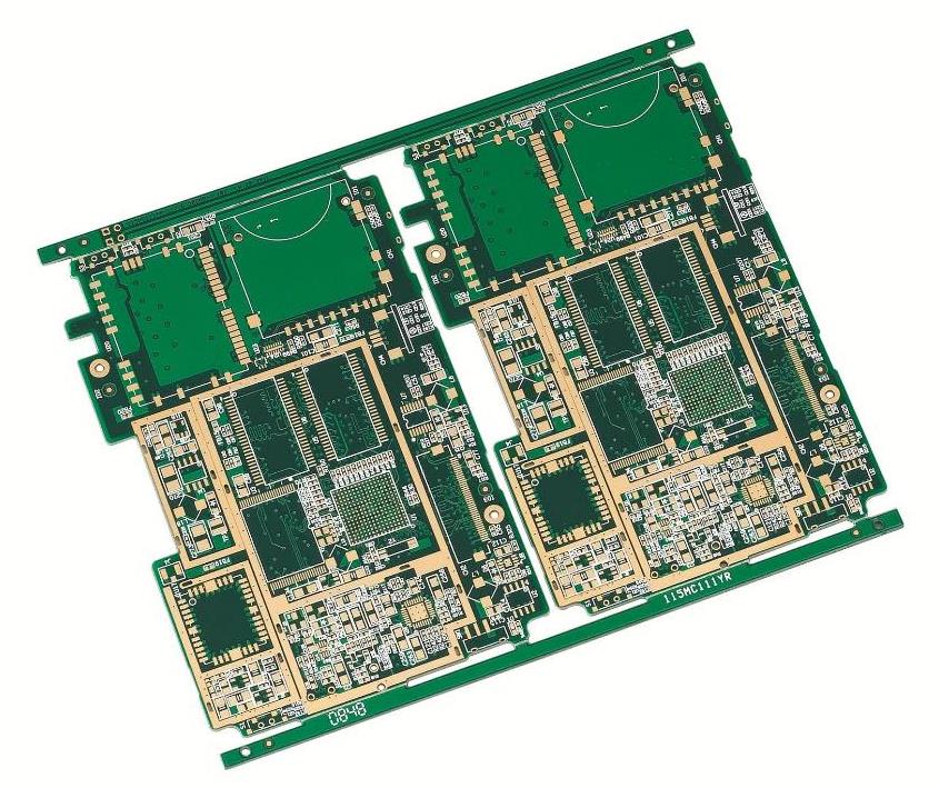
Four-layer circuit board, multi-layer circuit board, PCB board factory-multi-layer circuit board design suggestions
Multi-layer circuit boards are a special kind of printed circuit board, and its existence "place" is usually quite special. For example, there will be multi-layer circuit boards in the circuit board. This kind of multi-layer board can help the machine to conduct various different circuits, not only that, but also have the effect of insulation, will not let electricity and electricity collide with each other, and it is completely safe. If you want to use a better performance PCB multilayer board, you must concentrate on presetting, and then I will explain how to pre-set the multilayer circuit board.
One, PCB board shape, size and number of layers are confirmed
1. The number of layers must be determined according to the requirements of circuit performance, board size and the density of the circuit. For multilayer printed boards, the four-layer and six-layer boards are the most widely used. Taking the four-layer board as an example, there are two conductor layers (component surface and soldering surface), a power layer and a ground layer.
2. The layers of the multi-layer circuit board should be symmetrical, and it is best to have an even number of copper layers, that is, a four-layer circuit board, a six-layer PCB, an eight-layer circuit board, etc. Due to the wrong name of the lamination, the appearance of the PCB circuit board is prone to warping, especially the PCB multilayer circuit board that is mounted on the external surface, which should attract attention.
3. No matter what a printed circuit board, there is a problem of proper assembly with other structural parts. Therefore, the shape and size of the printed circuit board must be based on the structure of the product. But from the perspective of production technology, we should try our best to be simple. Generally, it is a rectangle with a length-to-width ratio that is not very different, so as to facilitate assembly to increase the production rate and reduce labor costs.

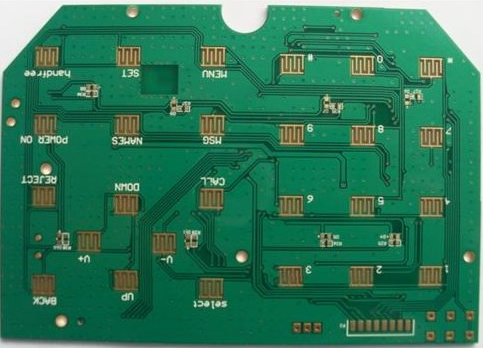
2. The location of the components and the placement direction of the pendulum
1. On the other hand, the problem should be considered from the group structure of the printed circuit board to prevent the uneven arrangement of the components and the reverse. This not only affects the good-looking of printed boards, but also brings many inconveniences to assembly and maintenance office.
2. The position of the components and the direction of the placement should first be considered from the circuit principle to cater to the direction of the circuit. Whether the placement of the pendulum is reasonable or not will directly affect the performance of the printed board, especially the high-frequency analog circuit, which makes the location and placement of the components more stringent.
3. Reasonable placement of components, in a sense, has shown the success of the printed board preset. Therefore, when starting to edit the layout of the printed board and the layout of the voting group, a thorough analysis of the circuit principle should be performed, and the location of special components (such as large-scale ICs, high-power tubes, signal sources, etc.) should be confirmed first, and then Place other components and try to prevent possible interference factors.
Three, wire layout, wiring area requirements
Under normal circumstances, the wiring of multilayer printed circuit boards is implemented according to circuit functions. When wiring on the outer layer, more wiring is required on the soldering surface and less wiring on the component surface, which helps the maintenance and troubleshooting of the printed board. Signal lines with thin and dense wires that are mildly disturbed are generally placed on the inner layer. The copper foil with the size of the large plane or the surface of the object should be more evenly dispersed in the inner and outer layers, which will help reduce the warpage of the board, and also make the surface of the electroplating obtain a more even coating. In order to avoid the appearance processing damage the printed wires and the interlayer short circuit caused by the mechanical processing, the distance between the conductive pattern of the inner and outer layer wiring area and the board edge should be greater than 50mil.
Fourth, the wire direction and line width requirements
Multilayer circuit board wiring should separate the power layer, ground layer and signal layer to reduce the interference between power, ground and signal. The lines of two adjacent layers of printed boards should try their best to be vertical to each other or follow diagonal lines or curves. Two non-intersecting straight lines should not be used to reduce the interlayer coupling and interference of the substrate. And the wires should try their best to go as short as possible, especially for small signal circuits. The shorter the wire, the smaller the resistance and the smaller the interference. For signal lines on the same layer, avoid sharp corners when changing directions. The width of the wire should be confirmed according to the current and impedance requirements of the circuit. The power input wire should be larger, and the signal wire can be relatively small. For ordinary digital boards, the power input line width can be deemed appropriate and use 50-80 mils, and the signal line width can be deemed appropriate and use 6-10 mils.
Wire width: 0.5, 1, 0, 1.5, 2.0; allowable current: 0.8, 2.0, 2.5, 1.9; wire resistance: 0.7, 0.41, 0.31, 0.25; pay attention to the width of the lines to be exactly the same when wiring, to prevent wires It suddenly becomes thicker and suddenly becomes thinner, which helps the impedance match.
5. Drilling volume and land requirements
1. The drilling volume of the component on the multilayer circuit board is related to the size of the selected component pin. If the drilling is too small, it will affect the assembly and tinning of the component; the drilling is too large, and the solder joints are not enough during soldering. full. Generally speaking, the calculation method of component hole diameter and pad volume is:
2. The aperture of the component hole = the component pin diameter (or diagonal) + (10~30mil)
3. The diameter of the component pad ≥ the diameter of the component hole + 18mil 4. As for the via hole diameter, it is mainly voted by the thickness of the finished board. For high density multilayer circuit boards, it should generally be restricted to the range of board thickness: aperture ≤ 5:1 Inside.
4. The calculation method of the via pad is: the diameter of the via pad (VIAPAD) ≥ the diameter of the via + 12mil.
Six, power layer, stratum division and flower hole requirements
For multilayer printed boards, there is at least one power layer and one ground layer. Because all the voltages on the printed circuit board are connected to the same power layer, it is necessary to implement partition isolation on the power layer. The volume of the partition line is generally considered appropriate and the line width of 20-80 mil is appropriate. The voltage is super high, and the partition line The thicker.
Welding holes are connected to the power layer and stratum. In order to increase its reliability and reduce the heat absorption of large and small metals on the surface or surface of the welding process, virtual welding occurs. The common connection plate should be preset to a flower hole pattern.
Isolation pad aperture ≥ drilling aperture+20mil
Seven, the requirements of the safety distance The setting of the safety distance should satisfy the requirements of electrical safety
Generally speaking, the minimum spacing of the outer conductors cannot be less than 4mil, and the minimum spacing of the inner conductors cannot be less than 4mil. In the case where the wiring can be arranged, the spacing should be as large as possible to increase the yield during board manufacturing and reduce the hidden danger of failure of the finished board.
8. Increase the anti-jamming experience of the entire board and require the preset of multi-layer printed boards, and be sure to pay attention to the anti-jamming experience of the entire board. Common methods are:
1. Choose a reasonable grounding point.
2, add filter capacitors near the power and ground of each IC, the volume is generally 473 or 104.
3. For sensitive signals on the printed circuit board, do not add accompanying shielded wires, and try to minimize wiring near the signal source.