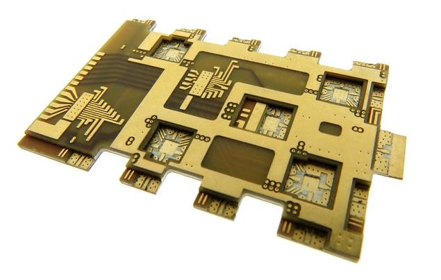
In recent years, due to the rapid growth of the market for Bluetooth devices, wearable devices, wireless local area network devices and mobile devices, the demand for RF circuits is also increasing. Especially in the next few years, the market for RF circuits will become more It is growing rapidly. However, the design of RF circuits is the same as electromagnetic interference, which has always been the most difficult problem for engineers to solve. If you want to successfully design a good RF circuit, you must carefully plan every step and detail in the entire design process, so as to win steadily.
There are many theoretical differences between the design of radio frequency PCB and the design of ordinary PCBs. First of all, there is uncertainty in radio frequency circuits, but this does not prevent us from being able to design a good radio frequency circuit. In fact, in the design of radio frequency circuits, there are still many rules and techniques that can be used. But in the actual process, these rules and techniques may be unusable due to certain restrictions, so how to deal with this problem has become an important problem in the RF design course.
In the development of wireless products, RF circuit wiring is a very critical element. It may be perfect in the design of the principle, but in reality there will always be some problems that restrict the performance of this circuit. In the actual test, the ideal state cannot be achieved, and many of these problems are the reasons for the incompleteness of the wiring process. Now we will cut into the problem of wiring to explain some tips that need to be paid attention to in the design of radio frequency PCB.
First of all, before wiring, we have to determine the structure of the PCB board, just like before building a house, we have to plan the number of layers of the house. The structure of the battery panel is related to the complexity of the PCB design, electromagnetic compatibility and many other factors. In the actual production design, there will be no single-layer board, so let's take a multilayer board as an example.
For example, for a four-layer board, the second layer is generally used as a complete ground plane in the design, and important signals are distributed on the top layer. In this way, the impedance can be well controlled. In the design of six-layer boards and more, all are the same as the design of four-layer boards. They all need a complete ground plane, and then use the top layer for signal routing.

Control impedance
What you need to pay attention to during the wiring process is to control the impedance. For example, when wiring, you should try to control the characteristics of the wiring to be 50Ω, and the resistance is related to the line width. When performing the principle design and simulation, you should use the formula to calculate the characteristic impedance at 50Ω. Up and down, the one that meets the requirements can be designed as a radio frequency trace.
Component placement
In PCB design, we generally follow a rule, that is, the traces are as short as possible, that is to say, the components are generally close to the power supply, and then the corresponding components are closely arranged. This not only ensures the beauty and clarity of the PCB board, but also shortens the length of the wiring. When designing the radio frequency circuit, we should also follow this design rule.
RF routing
When wiring, in addition to the length mentioned above, the length should be as short as possible. Another difference from ordinary PCB design is that the RF circuit wiring should be arc-shaped to achieve corners instead of the general 45°/135° corner. Because the RF signal line cannot have any inflection points. If the RF signal line has an unavoidable cross in the actual process, then it is necessary to use vias to guide a part of the signal for transmission. This part of the signal, whether it is on the bottom layer or the middle layer, the video routing A reference plane must be required. But it must be noted that the ground plane must be continuous.