Analysis of common preventive measures against ESD in PCB board design
The static electricity in the human body, the environment, and even electronic equipment can cause various damages to specific semiconductor chips, for example, infiltrating the insulating layer into the components; destroying the doors of Mosfet and CMOS components.
Trigger in CMMOS peripherals; short loop biased PN junction; direct differentiated pn connection; melting of solder wires or aluminum in the active device.
In order to eliminate the interference and destruction of the ionizing charge (ESD) of electronic equipment, various technical measures must be taken to prevent these charges.
This document provides the design of anti-static discharge printed circuit (ESD), which includes over-location, correct layout, wiring and installation.
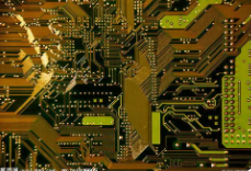
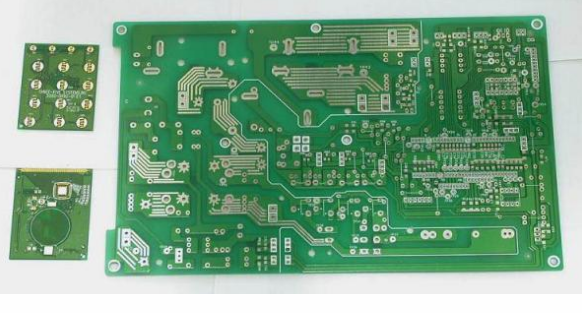
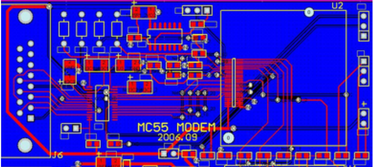
(1) Stacking By using the multilayer printed circuit board as much as possible, as an important load source of the multilayer PCB the surface of the ground can compensate the load of the electrostatic discharge source, thereby reducing the problems caused by the electrostatic field. The quality surface of the printed circuit can also be used as a shield for the signal line (of course, the greater the degree of openness on the proton surface, the greater the efficiency of protection). In addition, if discharged, the load can be easily injected into the surface of the printed circuit board instead of in the signal line. This will help protect the components, because the charge can be removed before the components are damaged. Of course, in order to reduce the cost in some systems, only double-layer boards can be used.

(2) Loop The induced current on the PCB board, the circuit loop is closed and has a variable magnetic current. The magnitude of the current is proportional to the surface of the ring. A larger ring contains more magnetic flux, which generates a higher current in the circuit. Therefore, the area of the loop must be reduced.
(3) Circuit connection length Please make sure that the signal line is as short as possible. In order to make the antenna highly efficient, its length must be a large part of the wavelength. This means that a longer line will help to receive the frequency components generated by the EDD pulse, while a shorter line will only get fewer frequency components.
Therefore, the energy of the electromagnetic field generated from the electrostatic discharge of the short conductor is reduced to the power supply in the circuit. When the length of the signal line exceeds 300 mm (12 inches), a parallel quality line is required.
It is also possible to provide a proton line on the signal line or its adjacent surface. In the appropriate component group, there are many interconnected parts that must be close to each other. For example, the E/S peripherals are as close as possible to the E/S connector to reduce the length of the interconnect printed circuit.
(4) Ground load ejection Direct discharge of electrostatic landfills on the ground may damage sensitive circuits. In addition to the use of TVS diodes, one or more high-frequency derivative capacitors are used, which are placed between the vulnerable parts and the power supply between the earth. The bypass capability reduces charge injection and maintains the voltage difference between the power supply and the ground connection port. TVS maintains inductance and maintains the potential difference of the TVs blocking voltage. TVS and capacitors should be as close as possible to the protected integrated circuit. In order to reduce the parasite inducing effect, the shortest length and the slice of the capacitor on the TVS channel must be ensured.
(5) Parasitic inductance in the protection circuit When an ESD event occurs, the parasitic inductance in the path of the TVS diode can cause a serious voltage overshoot. Although the induced voltage of VL = l * di / DT is used at the two ends of the inductive inductor, over-boosting may always exceed the damage voltage threshold of the protected integrated circuit. The total voltage of the protection circuit is the sum of the voltage generated by the blocking voltage of the Tvs diode, VT = vC + vl. A transitional induced current reaches its maximum value in less than 1 second (according to the IEC 61000-4-2 standard). Assuming that the inductance of the probe is 20 nnhh per inch and the line length is a quarter, the overvoltage will be 50V / Pulse 10a. Make the derivative as short as possible to reduce the effect of parasitic inductance.
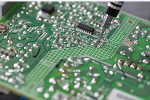
(6) Assembly When assembling the PCB board, no soldering is applied on the upper or lower level. Screws with integrated seals can establish close contact between the printed circuit and the metal liner/shield, or maintain close contact on the correction surface. The same "isolation zone" must be determined between the quality of the chassis and the quality of the circuits on each layer. If possible, maintain a distance of 0.64 mm (0.0025 inch). On the map and downstairs, near the installation hole, the floor of the wardrobe and the circuit are connected in the wardrobe by a 1.27 mm wide (0.0050 inch) yarn, every 100 mm (4.0 inch).
Place the wooden dices or assembly holes between the closet and the ground of the circuit board where these connection points are adjacent. These ground connections can be connected to the blade to maintain an open circuit or have high frequency PCB/capacitor magnetic bounce to change the mechanism used for the ground in ESD testing.