How to use Altium designer software to design multilayer PCB boards
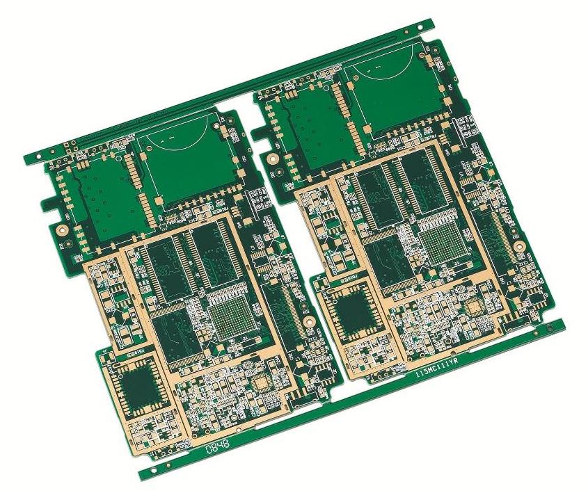
PCB multi-layer boards are more complicated in terms of applications and circuits, high-frequency boards, and high-frequency signals. Compared with double-layer or single-layer boards, the production cost is higher.
However, with regard to signal integrity, interference prevention and other aspects, the design of multi-level maps is not difficult, but there are some additional layers inside, mainly wiring and wiring.
The commonly used EDA circuit can be designed with multi-layer printed circuit boards, although the methods are different, the principles are the same. This is how to apply Alterer designers in the process of designing multilayer printed circuit boards.
The software used here is F17 version. If you use another version, some steps will be slightly different and cannot be copied. The software used is the most important. Start the software. New PCB project.
Document-New-PCB The normal approach is to first establish a new design workspace or a new PCB project. Here, there is only a new PCB file to show how to design a multi-layer map.
Therefore, there is no need to set up a new project.

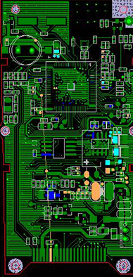
Design (design)-stack layer manager (layer management), open layer management. This is the 17th edition of the management interface of the curling ear layer.
Please note the differences between other versions, for example, a layer of management interface. In the card management, there are two cards on the top and two cards on the bottom. If you need a multi-layer card, you can use the following method.
1. Insert the inner layer. The internal layer and the entire plan, all copper coating, negative corrosion corrosion, that is, on the anti-corrosion line, can be used as a layer or layer.
2. Add an intermediate layer.
The intermediate layer can be used as routing, which is different from the ordinary signal layer, but routing is included. This is a positive corrosion.
The order of the power layer or the ground layer and the signal layer can be divided into top layer-power layer-ground layer-bottom layer; top layer-ground layer-power layer-bottom layer.
The top and bottom layers are mainly signal layers, and the inner electrical layers in the middle are power and ground layers.
If you add an inner layer, please point to the top, add an inner lining in the lower left corner of the card management, plus an inner plan, you can add underwear, you can layer the underwear, such as layering, or it can be deleted.
When adding the inner layer, the thickness and material of the layer should be filled as needed.
Sight. On the keyboard, you can see the signal layer and the inner layer.
Additional layers and other layers can also be seen in the layered allocation column under the software.
After adding a layer, you can draw the shape of the PCB board and frame, and then import the network station, layout, and wiring.