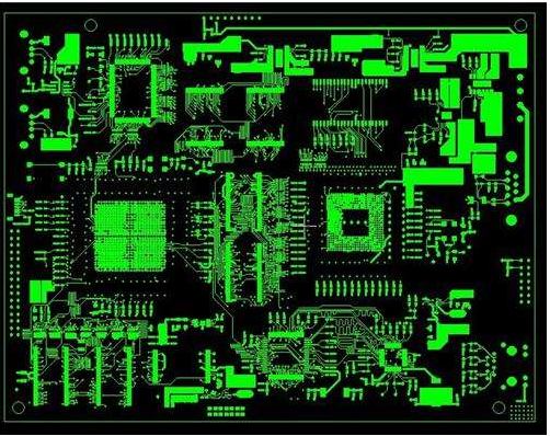
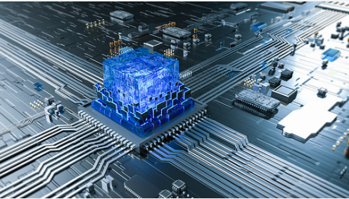
The printed circuit board design process includes drawing circuit schematics, planning printed circuit boards, component packaging, component layout, automatic wiring, manual adjustment, saving output, etc. The following is the design flow of the printed circuit board.

(1) Principles of drawing circuit diagrams.
This is the basis of circuit board design, mainly to complete the drawing of circuit schematics and generate network reports.
(2) Planning the circuit board.
Before drawing the circuit board, the user should make a preliminary plan for the circuit board, including setting the physical size of the circuit board, adopting several layers of circuit boards, component packaging and installation, etc. This determines the framework for the subsequent printed circuit board design.
(3) Set parameters.
It is mainly to set the distribution parameters and wiring parameters of the components. Usually these parameters can be selected from the default values of the system, or there is no need to modify them after setting them once.
(4) Component packaging.
The so-called component packaging is the shape of the component, and each component installed on the printed circuit board should have a corresponding package, so as to ensure the normal wiring of the circuit board.
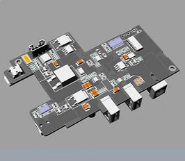
(5) Component layout.
After the circuit board is planned, the components can be placed in the circuit board frame, and the automatic wiring function provided by protel 99 SE can be used to automatically route the components.
(6) Automatic wiring
Protel 99 SE provides a powerful automatic wiring function, which can automatically route the arranged components. Under normal circumstances, automatic wiring will not go wrong.
(7) Manual adjustment
After the automatic wiring is completed, the user can adjust the more special components to ensure compliance with the corresponding rules, so as to ensure that the anti-interference of the circuit board reaches the standard.
(8) Save the output.
After wiring the components and making correct adjustments, the final design of the printed circuit board is completed, and then the drawings are printed and the output is saved.
The above is an introduction to the design methods and steps of printed circuit boards. Ipcb also provides PCB manufacturing and PCB manufacturing methods.