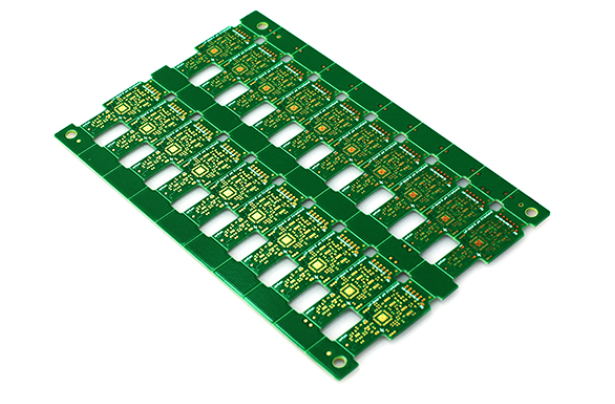
Two common PCB board imposition designs
1. V-groove imposition design
V-Groove imposition connection method is suitable for imposition of board thickness ≥1.0mm and PCB (daughter board) sides are straight lines. PCB board thickness<1.0mm is not suitable for V-groove imposition method, because the thinner the PCB, the smaller the depth of the V-groove. The board will bend and it is easy to damage the components.
【Design requirements】
(1) The general design requirements for the shape and size of the V-shaped groove are as follows:
The remaining thickness is generally 1/3 of the thickness of the plate, and the minimum is 0.40mm;
The angle of the V-shaped groove is 30°~45°, and 30° is recommended;

The misalignment of the cuts on the upper and lower sides of the V-shaped groove should be<0.13mm
(2) The height limit of the components on both sides of the V-shaped groove: within 5mm from the V-shaped groove, the device height is less than 27mm; within the range of 5-20mm from the V-shaped groove, the height of the device is less than 35mm.
(3) The wire or copper skin should be more than 1.0mm away from the edge of the V-groove to avoid damage to the conductor during board splitting.
【Remark】
The residual thickness of the V-groove processing should be determined according to the plate thickness to ensure good plate separation and welding. If there are stress-sensitive components (such as chip capacitors, BGA, etc.) installed on the PCB of the unit, manual splitting is not recommended, and machine splitting should be used.
There are two types of V-groove splitting machines, namely front and rear board feeding (2M) and left and right board feeding (4M). The former has PCB movement, which is prone to board deflection and poor stress stability; the latter has good manufacturability and does not move the PCB. .
The strain direction of the V-groove manual sub-plate is perpendicular to the direction of the V-groove, while the strain direction of the machine sub-plate is usually at an angle of 30°~45° with the direction of the V-groove, so the requirements for the component layout direction are different.
2. Stamp hole imposition design
The stamp hole imposition connection method, that is, the connection method of the long slot and the stamp hole, is used for the imposition of various shapes of sub-boards. The design parameters mainly include the size of the long groove and the aperture and spacing of the stamp.
【Design requirements】
(1) The groove width is generally 1.6~3.0mm, and the recommended value is 2.4mm; the groove length should be ≤50mm; the width of the connecting bridge between the groove and the groove is designed according to the required size of 5 holes or 7 holes.
(2) The hole diameter of the stamp is Ø0.8mm; the hole center distance is generally the hole diameter plus 0.4mm~0.6mm, the thickness of the plate is the smaller value, and the thickness of the plate is the larger value.
(3) The semicircle at both ends of the long groove is tangent to or connected to the stamp hole.
(4) The maximum distance between the connecting bridge and the corner is 12.5mm.
(5) The wire or copper skin should be more than 1.5mm away from the edge of the stamp hole to avoid damage to the conductor when dividing the board.
【Remark】
The stamp hole connection method is a more commonly used imposition connection method, which is suitable for PCBs with regular and irregular shapes.
With the increase in component layout density, the layout of components is getting closer and closer to the dividing edge. In order to avoid damage to nearby components due to stress during board splitting, the splitting process of mechanical milling is adopted. In this case, the existence of stamp holes is meaningless, and a long slot connection method is derived, which has high connection strength., It is widely used in the imposition design of thin plates. The disadvantage is that it requires a special milling splitter to split the board.
ipcb is a high-precision, high-quality PCB manufacturer, such as: isola 370hr PCB, high-frequency PCB, high-speed PCB, ic substrate, ic test board, impedance PCB, HDI PCB, Rigid-Flex PCB, buried blind PCB, advanced PCB, microwave PCB, telfon PCB and other ipcb are good at PCB manufacturing.