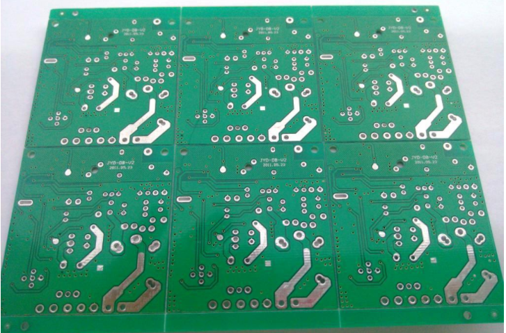
The big difference between a conventional PCB and a backplane lies in the size and weight of the board, as well as the processing of large and heavy raw material panels. The standard size of PCB manufacturing equipment is typically 24x24 inches. However, users, especially telecommunication users, require larger backplanes. This has promoted the confirmation and purchase of large-size board conveying tools. Designers have to add additional copper layers to solve the routing problem of the large-pin-count connector, which increases the number of backplane layers. The harsh EMC and impedance conditions also require an increase in the number of layers in the design to ensure adequate shielding, reduce crosstalk, and improve signal integrity.

When a card with high power consumption is inserted into the backplane, the thickness of the copper layer must be moderate to provide the required current to ensure that the card can work normally. All these factors lead to an increase in the average weight of the backplane, which requires that conveyor belts and other conveying systems must not only be able to safely transfer large-size raw boards, but also must take into account the fact that their weight has increased.
The user's need for a thinner layer core and a more layered backplane brings about two opposite requirements for the conveying system. Conveyor belts and conveying devices must be able to pick up and transport large-format thin plates with a thickness of less than 0.10 mm (0.004 inches) without damage on the one hand, and must also be able to transport 10 mm (0.394 inches) thick and 25 kg (56 pounds) weight on the other hand. The board does not fall off the board.
The difference between the thickness of the inner plates (0.1mm, 0.004 inches) and the thickness of the final backplane (up to 10mm, 0.39 inches) is two orders of magnitude, which means that the conveying system must be strong enough to safely transport them Transfer through the processing area. Since the backplane is thicker than the conventional PCB and the number of holes is much larger, it is easy to cause the process fluid to flow out. The 10mm thick back plate with 30,000 holes can easily take out a small amount of working fluid that is adsorbed in the guide hole by surface tension. In order to minimize the amount of liquid carried and eliminate the possibility of any drying impurities remaining at the guide hole, it is extremely important to clean the borehole by means of high pressure flushing and air blower.
layer counterpoint
As user applications require more and more board layers, the alignment between layers becomes very important. Interlayer alignment requires tolerance convergence. The board size has become more demanding for this convergence requirement. All layout processes are produced in a certain temperature and humidity controlled environment. The exposure equipment is in the same environment, and the alignment tolerance of the front image and the back image of the entire area must be maintained at 0.0125mm (0.0005 inch). In order to achieve this accuracy requirement, a CCD camera needs to be used to complete the alignment of the front and rear layout.
After etching, use a four-drilling system to perforate the inner plate. The perforation passes through the core plate, the position accuracy is maintained at 0.025mm (0.001 inch), and the repeatability is 0.0125mm (0.0005 inch). Then insert a pin into the perforation to align the etched inner layer while bonding the inner layer together.
In the beginning, the use of this post-etching perforation method can fully ensure the alignment of the drilled hole and the etched copper plate, forming a solid ring-shaped design structure. However, as users require more and more circuits to be laid in a smaller area in terms of PCB routing, in order to keep the fixed cost of the board unchanged, the size of the etched copper plate is required to be smaller, and the interlayer copper plate is required to be better Counterpoint. To achieve this goal, an X-ray drilling machine can be purchased. The device can drill a hole on a large size board of 1092*813mm (43*32 inches) with a position accuracy of 0.025mm (0.001 inch). There are two usages:
1. Use an X-ray machine to observe the etched copper on each layer, and determine a good position with the help of drilling holes.
2. The drilling machine stores statistical data and records the deviation and divergence of the alignment data relative to the theoretical value. This SPC data is fed back to the previous processing procedures, such as the selection of raw materials, processing parameters and layout drawing, etc., to help reduce the rate of change and continuously improve the process.
Although the electroplating process is similar to any standard plating process, due to the unique characteristics of the large-scale backplane, there are two main differences that must be considered.
Fixtures and conveying equipment must be able to convey large-size boards and heavy boards at the same time. The weight of a large-format raw material substrate of 1092x813mm (43x32 inches) can reach 25 kilograms (56 pounds). The substrate must be able to be securely gripped during transportation and processing. The design of the tank must be deep enough to accommodate the board, and uniform plating characteristics must be maintained throughout the tank.
In the past, users all specified press-fit connectors for backplanes, so they relied too heavily on the uniformity of copper plating. The thickness of the backplane produces a variation of 0.8 mm to 10.0 mm (0.03 inches to 0.394 inches). The existence of various aspect ratios and larger substrate specifications make the uniformity index of electroplating become critical. In order to achieve the required uniformity, periodic reverse ("pulse) plating control equipment must be used. In addition, the necessary stirring must be performed to keep the plating conditions as uniform as possible.
In addition to the uniform thickness of the plating layer required for drilling, backplane designers generally have different requirements for the uniformity of copper on the outer layer surface. Some designs have very few signal lines etched on the outer layer. On the other hand, facing the demand for high-speed data rates and impedance control circuits, it will become necessary to install a nearly solid copper sheet on the outer layer for EMC shielding.
detection
Since users require more layers, it is very important to ensure that defects are identified and isolated on the inner etched layer before bonding. In order to achieve effective and repeatable control of the backplane impedance, the etching line width, thickness and tolerance have become key indicators. At this time, the AOI method can be used to ensure the matching of the etched copper pattern with the design data. The impedance model is used to determine and control the sensitivity of impedance to line width changes by setting the line width tolerance on the AOI.
Large-size and multi-drilled backplanes and the trend of placing active circuits on the backplane have jointly promoted the need for strict inspection of bare boards before component loading for efficient production.
The increase in the number of holes on the backplane means that the bare board test fixture will become very complicated, although the use of a dedicated fixture can greatly shorten the unit test time. In order to shorten the production process and prototype manufacturing time, the double-sided flying probe detection fixture is used and the original design data is used for programming, which can ensure the consistency with the user's design requirements, reduce costs and shorten the time to market.
The above is the main points of PCB backplane design and testing. Ipcb is also provided to PCB manufacturers and PCB manufacturing technology