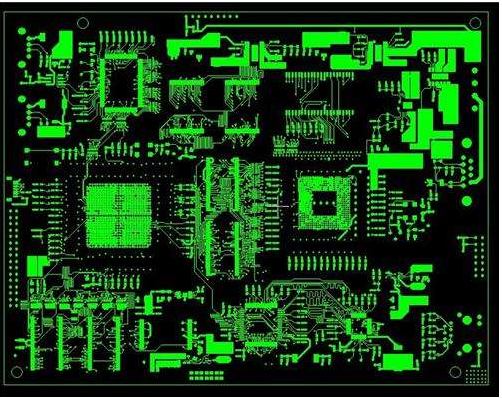
In circuit board design, wiring is an important step to complete product design. It can be said that the previous preparations are done for it. In the entire PCB, the wiring design process is the highest limit, the skills are the smallest, and the workload is the largest. PCB wiring includes single-sided wiring, double-sided wiring and multilayer wiring. There are also two ways of wiring: automatic wiring and interactive wiring. Before automatic wiring, you can use interactive to pre-wire the more stringent lines. The edges of the input end and the output end should be avoided adjacent to parallel to avoid reflection interference. If necessary, ground wire should be added for isolation, and the wiring of two adjacent layers should be perpendicular to each other. Parasitic coupling is easy to occur in parallel.
The layout rate of automatic routing depends on a good layout. The routing rules can be preset, including the number of bending of the wiring, the number of vias, the number of steps, and so on. Generally, explore the warp wiring first, quickly connect the short wires, and then perform the labyrinth wiring. First, the wiring to be laid is optimized for the global wiring path. It can disconnect the laid wires as needed. And try to re-wire to improve the overall effect.
The current high-density PCB design has felt that the through-hole is not suitable, and it wastes a lot of valuable wiring channels. In order to solve this contradiction, blind and buried hole technologies have emerged, which not only fulfill the role of the through-hole It also saves a lot of wiring channels to make the wiring process more convenient, smoother and more complete. The PCB board design process is a complex and simple process. To master it well, a vast electronic engineering design is required. Personnel can get the true meaning of it only by experiencing it by themselves.

1 Treatment of power supply and ground wire
Even if the wiring in the entire PCB board is completed very well, the interference caused by the improper consideration of the power supply and the ground wire will reduce the performance of the product, and sometimes even affect the success rate of the product. Therefore, the wiring of the electric and ground wires must be taken seriously, and the noise interference generated by the electric and ground wires should be minimized to ensure the quality of the product.
Every engineer engaged in the design of electronic products understands the cause of the noise between the ground wire and the power wire, and now only the reduced noise suppression is described:
(1) It is well-known to add decoupling capacitors between the power supply and ground.
(2) Widen the width of the power and ground wires as much as possible, preferably the ground wire is wider than the power wire, their relationship is: ground wire>power wire>signal wire, usually the signal wire width is: 0.2~0.3mm, the thinnest The width can reach 0.05~0.07mm, and the power cord is 1.2~2.5 mm. For the PCB of the digital circuit, a wide ground wire can be used to form a loop, that is, to form a ground net to use (the ground of the analog circuit cannot be used in this way)
(3) Use a large area of copper layer as the ground wire, and connect the unused places on the printed board to the ground as the ground wire. Or it can be made into a multilayer board, and the power supply and ground wires occupy one layer each.
2 Common ground processing of digital circuit and analog circuit
Many PCBs are no longer single-function circuits (digital or analog circuits), but are composed of a mixture of digital and analog circuits. Therefore, it is necessary to consider the mutual interference between them when wiring, especially the noise interference on the ground wire.
The frequency of the digital circuit is high, and the sensitivity of the analog circuit is strong. For the signal line, the high-frequency signal line should be as far away as possible from the sensitive analog circuit device. For the ground line, the whole PCB has only one node to the outside world, so The problem of digital and analog common ground must be dealt with inside the PCB, and the digital ground and analog ground inside the board are actually separated and they are not connected to each other, but at the interface (such as plugs, etc.) connecting the PCB to the outside world. There is a short connection between the digital ground and the analog ground. Please note that there is only one connection point. There are also non-common grounds on the PCB, which is determined by the system design.
3 Wiring processing of signal lines in the electrical (ground) layer
When the signal line is laid on the electrical (ground) layer and the multilayer printed board is laid out, there are not many wires left in the signal line layer that have not been laid out. Adding more layers will cause waste and increase production. The workload and cost have also increased accordingly. To solve this contradiction, you can consider wiring on the electrical (ground) layer. The power layer should be considered first, and the ground layer second. Because it is best to preserve the integrity of the formation.
4 Treatment of connecting legs in large area conductors
In large-area grounding (electricity), the legs of common components are connected to it. The treatment of the connecting legs needs to be considered comprehensively. In terms of electrical performance, it is better to connect the pads of the component legs to the copper surface. There are some undesirable hidden dangers in the welding and assembly of components, such as: 1. Welding requires high-power heaters. 2. It is easy to cause virtual solder joints. Therefore, both electrical performance and process requirements are made into cross-patterned pads, called heat shields, commonly known as thermal pads (Thermal), so that virtual solder joints may be generated due to excessive cross-section heat during soldering. Sex is greatly reduced. The processing of the power (ground) leg of the multilayer board is the same.
5 The role of the network system in cabling
In many CAD systems, wiring is determined by the network system. The grid is too dense and the path has increased, but the step is too small, and the amount of data in the field is too large. This will inevitably have higher requirements for the storage space of the device, and also the computing speed of the computer-based electronic products. Great influence. Some paths are invalid, such as those occupied by the pads of the component legs or by mounting holes and fixed holes. Too sparse grids and too few channels have a great impact on the distribution rate. Therefore, there must be a well-spaced and reasonable grid system to support the wiring.
The distance between the legs of standard components is 0.1 inches (2.54 mm), so the basis of the grid system is generally set to 0.1 inches (2.54 mm) or an integral multiple of less than 0.1 inches, such as: 0.05 inches, 0.025 inches, 0.02 Inches etc.
6 Design Rule Check (DRC)
After the wiring design is completed, it is necessary to carefully check whether the wiring design conforms to the rules formulated by the designer, and it is also necessary to confirm whether the established rules meet the requirements of the printed board production process. The general inspection has the following aspects:
(1) Whether the distance between line and line, line and component pad, line and through hole, component pad and through hole, through hole and through hole is reasonable, and whether it meets the production requirements.
(2) Is the width of the power line and the ground line appropriate, and is the power supply and the ground line tightly coupled (low wave impedance)? Is there any place in the PCB where the ground wire can be widened?
(3) Whether the best measures have been taken for the key signal lines, such as the shortest length, the protection line is added, and the input line and output line are clearly separated.
(4) Whether there are separate ground wires for the analog circuit and digital circuit.
(5) Whether the graphics (such as icons and annotations) added to the PCB will cause signal short circuit.
(6) Modify some unsatisfactory linear shapes.
(7) Is there a process line on the PCB? Whether the solder mask meets the requirements of the production process, whether the solder mask size is appropriate, and whether the character logo is pressed on the device pad, so as not to affect the quality of the electrical equipment.
(8) Whether the outer frame edge of the power ground layer in the multilayer board is reduced. For example, the copper foil of the power ground layer is exposed to the outside of the board and it is easy to cause a short circuit.