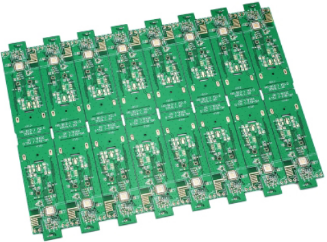
PCB structure design. In this step, according to the printed circuit board size and mechanical positioning, PCB board surface is drawn in the PCB design environment, and connectors, buttons/switches, screw holes, assembly holes and so on are placed according to positioning requirements. And fully consider and determine the wiring area and non-wiring area (such as how much of the screw hole around the non-wiring area).
PCB layout. Layout is basically putting devices on a board. At this point, if all the preparatory work mentioned above is done, you can generate the Design- CreateNetlist on the schematic, and then import the network table Design- LoadNets on the PCB diagram. See the device hubbub of the whole pile up, between the pins and fly line prompt connection. You can then layout the device. The general layout is carried out according to the following principles:

How to draw PCB board in PCB design environment
(1). According to the electrical performance reasonable partition, generally divided into: digital circuit area (that is, afraid of interference, and interference), analog circuit area
(fear of interference), power drive area (interference source);
(2). Complete the same function of the circuit, should be placed as close as possible, and adjust the components to ensure simple connection; At the same time, adjust the relative position between the functional blocks to make the line between the functional blocks simple;
Wiring. Wiring is an important procedure in PCB design. This will directly affect the performance of PCB board. In the process of PCB design, wiring generally has such three levels of division: the first is the distribution, which is the basic requirement of PCB design. If the line is not cloth, get everywhere is flying line, it will be a unqualified board, can say that there is no entry. The second is the satisfaction of electrical performance. This is the standard to measure whether a printed circuit board is qualified. This is after the distribution, carefully adjust the wiring, so that it can achieve the electrical performance. Then there is aesthetics. If your wiring cloth was connected, also do not have the place that what affects electric appliance performance, but look past desultorily, add colourful, brightly colored, that calculates how your electric appliance performance is good, still be rubbish in others eye. This brings great inconvenience to testing and maintenance. Wiring should be neat and uniform, not crisscross without rules. All these should be achieved in the context of ensuring electrical performance and meeting other individual requirements, otherwise it is to abandon the essence.
Wiring optimization and screen printing. "There is no, only better"! No matter how much effort you put into the design, when you're done, look at it again, and you'll still feel you can change a lot. A general design rule of thumb is that optimal wiring takes twice as long as initial wiring. After feeling that nothing needs to be changed, Place- polygonPlane. Laying copper generally laying ground wire (pay attention to the separation of analog and digital ground), multilayer board may also need to lay power. For screen printing, we should pay attention to not be blocked by the device or removed by the hole and pad. At the same time, design to face the component surface, the bottom of the word should be mirror processing, so as not to confuse the level.
Network and DRC inspection and structural inspection. Firstly, on the premise that the schematic design is correct, the generated PCB network files and schematic network files are NETCHECK for physical connection relationship, and the design is timely amended according to the output file results to ensure the correctness of wiring connection relationship; After the network check is passed correctly, DRC check will be carried out on the PCB design, and the design will be amended according to the output file results in time to ensure the electrical performance of PCB wiring. Further inspection and confirmation of PCB mechanical installation structure is required.
Plate making. Before that, there is a review process. PCB design is a test of the mind of the work, who is close to the mind, high experience, the design of the board is good. So the design should be extremely careful, fully consider the factors of all aspects (such as facilitate maintenance and inspection of this a lot of people do not consider), excellence, will be able to design a good board.