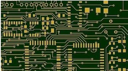
The PCB circuit board is the basic electronic component of all electronic circuit design, and the design of the PCB circuit board is also what small partners must understand. The role of PCB is not only to combine scattered components, but also to ensure the regularity of circuit design, and to avoid confusion and errors caused by manual wiring and wiring.
1. There must be a reasonable direction
Such as input/output, AC/DC, strong/weak signal, high frequency/low frequency, high voltage/low voltage, etc. Their direction should be linear (or separated) and must not blend with each other. Its purpose is to prevent mutual interference. The best trend is in a straight line, but it is generally not easy to achieve. The most unfavorable trend is a circle. Fortunately, isolation can be set to improve. For DC, small signal, low voltage PCB design requirements can be lower. So "reasonable" is relative.
2. Choose a good grounding point: the grounding point is often the most important
A small grounding point, I don’t know how many engineers and technicians have talked about it, which shows its importance. Under normal circumstances, a common ground is required, such as: multiple ground wires of the forward amplifier should be merged and then connected to the main ground, and so on. In reality, it is difficult to achieve this completely due to various restrictions, but we should try our best to follow it. This problem is quite flexible in practice. Everyone has their own set of solutions. It is easy to understand if they can explain it for a specific circuit board.

3. Reasonably arrange power filter/decoupling capacitors
Generally, only a number of power filter/decoupling capacitors are drawn in the schematic diagram, but it is not pointed out where they should be connected. In fact, these capacitors are set up for switching devices (gate circuits) or other components that require filtering/decoupling. These capacitors should be placed as close as possible to these components. If they are too far away, they will have no effect. Interestingly, when the power supply filter/decoupling capacitors are arranged properly, the problem of the grounding point becomes less obvious.
4. There is a requirement for the line diameter to be a suitable buried hole through hole size
If conditions permit, wide lines should never be thin; high-voltage and high-frequency PCB lines should be round and slippery, without sharp chamfers, and corners should not be at right angles. The ground wire should be as wide as possible, and it is best to use a large area of copper, which can greatly improve the problem of grounding points. The size of the pad or via is too small, or the size of the pad and the hole size are not properly matched. The former is unfavorable for manual drilling, and the latter is unfavorable for CNC drilling. It is easy to drill the pad into a "c" shape, but to drill off the pad. The wire is too thin, and the large area of the unwiring area is not provided with copper, which is easy to cause uneven corrosion. That is, when the unwiring area is corroded, the thin wire is likely to be over corroded, or it may appear to be broken, or completely broken. Therefore, the role of setting copper is not only to increase the area of the ground wire and anti-interference.
5. Number of vias, solder joints and line density
Some problems are not easy to be found in the early stage of circuit production. They tend to emerge in the later stage. For example, if there are too many vias, a slight mistake in the copper sinking process will bury hidden dangers. Therefore, the design should minimize the wire hole. The density of parallel lines in the same direction is too large, and it is easy to join together when welding. Therefore, the line density should be determined according to the level of the welding process. The distance of the solder joints is too small, which is not conducive to manual welding, and the welding quality can only be solved by reducing the work efficiency. Otherwise, hidden dangers will remain. Therefore, the minimum distance of solder joints should be determined by comprehensive consideration of the quality and work efficiency of the welding personnel.
If you can fully understand and master the above-mentioned PCB circuit board design precautions, you can greatly improve the design efficiency and product quality. Correcting the existing errors during production will save a lot of time and cost, and save rework time and material input.
Now PCB design time is getting shorter and shorter, smaller and smaller circuit board space, higher and higher device density, extremely demanding layout rules and large-size components make designers