Circuit board design of circuit board and auxiliary side connection design
1 V-CUT connection
1: When the board is connected in a straight line, and the edge is flat and does not affect the device installation, this type of connection can be used for the PCB. The V-CUT is a straight-through type and cannot turn in the middle.
2: The recommended PCB thickness required by the V-CUT design is ≤3.0mm.
3: For PCBs that require automatic machine splitting, both sides of the V-CUT line (TOP and BOTTOM surfaces) are required to reserve a device forbidden area of not less than 1mm to avoid damage to the devices during automatic splitting.
V-CUT automatic PCB layout requirements
Within 5mm of the forbidden area from the edge of the board, it is not allowed to lay out devices with a device height higher than 25mm.
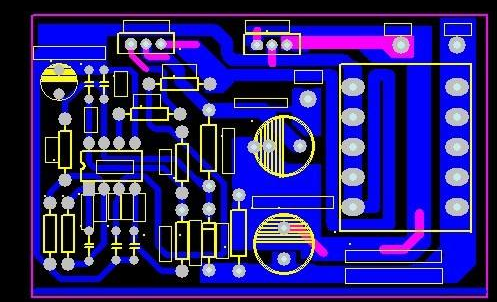
Requirement of automatic splitter blades for PCB edge devices
The above two need to be considered comprehensively when adopting V-CUT design, whichever is more stringent. Ensure that the components will not be damaged during the V-CUT process, and the board can be split freely.

At this time, the safety distance "S" from the edge of the V-CUT to the edge of the line (or PAD) should be considered to prevent the line from being damaged or exposed to copper. Generally, S≥0.3mm is required.
2 Stamp hole connection
[1] The recommended slot width is 2mm. Slot milling is often used when a certain distance is required between the unit boards, and is generally used in conjunction with V-CUT and stamp holes.
[2] The design of the stamp holes: the hole spacing is 1.5mm, and the recommended distance between the two sets of stamp holes is 50mm.
3 Imposition method
There are three recommended imposition methods: same direction imposition, center symmetric imposition, and mirror symmetric imposition.
[3] When the PCB unit board size is less than 80mm*80mm, it is recommended to do imposition;
[4] Designers need to consider the utilization rate of the board when designing the PCB board, which is one of the important factors affecting the cost of the PCB.
Note: For some irregular PCBs (such as L-shaped PCBs), using appropriate imposition methods can increase the utilization rate of the board and reduce the cost.
[5] If the PCB is to undergo reflow soldering and wave soldering processes, and the unit board width is >60.0mm, the number of impositions in the direction of the vertical conveying edge should not exceed 2.
[6] If the unit board size is very small, the number of impositions in the vertical conveying direction can exceed 3, but the total width perpendicular to the veneer conveying direction cannot exceed 150.0mm, and auxiliary tooling fixtures need to be added during production to prevent veneers Deformed.
[7] Same direction imposition
l Regular unit board
Use V-CUT imposition, if it meets the requirements of 4.1 cloth prohibition, imposition without auxiliary edge is allowed
Irregular cell board
When the shape of the PCB unit board is irregular or there are components beyond the board edge, the method of milling grooves and V-CUT can be used.
[8] Center symmetrical imposition
l Central symmetrical imposition is suitable for two PCBs with irregular shapes. Place the sides of the irregular shape in the middle to make the shape become regular after imposition.
l Irregularly shaped PCBs are symmetrical, and a slot must be milled in the middle to separate the two unit boards
l If the imposition produces a large deformation, you can consider adding auxiliary blocks between the impositions (connected with stamp holes)
[9] Mirror symmetrical imposition
Conditions of use: When the SMD on both the front and back of the unit board meets the requirements of reflow soldering on the back, mirror symmetry can be used.
Operation note: Mirror and symmetrical imposition must meet the symmetrical distribution of positive and negative films of PCB light painting. Take a 4-layer board as an example: if the second layer is the negative of the power/ground, the symmetrical third layer must also be the negative, otherwise mirror symmetry cannot be used.
After adopting mirror symmetry, the Fiducial mark of the auxiliary side must meet the requirements of overlap after flipping. For specific location requirements, please refer to the base point design of the imposition below.
4 Connection method of auxiliary side and PCB
[10] General principles
l When the device layout cannot meet the requirements of the width of the transmission edge (5mm forbidden area on the edge of the board), the method of adding auxiliary edges should be adopted.
l When there are missing corners or irregular shapes on the side of the PCB and cannot meet the requirements of the PCB shape, auxiliary blocks should be added to fill in, the period is regular, and it is convenient to assemble.
[11] Handling of vacancies on board edges and on board
When there is a gap on the edge of the board, or there is a gap larger than 35mm*35mm in the board, it is recommended to add an auxiliary block in the gap to facilitate the processing of SMT and wave soldering equipment. The connection between the auxiliary block and the PCB generally adopts the method of milling groove + stamp hole.