Six tips for selecting components in circuit board design
The best circuit board design method: Six things to consider when selecting circuit board components based on component packaging. All the examples in this article were developed using the Multisim design environment, but the same concepts still apply even with different EDA tools.
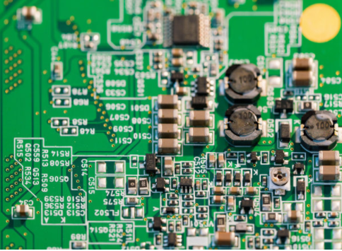
1. Consider the choice of component packaging
In the entire schematic drawing stage, you should consider the component packaging and land pattern decisions that need to be made in the layout stage. Some suggestions to consider when selecting components based on component packaging are given below.
. Remember, the package includes the electrical pad connections and mechanical dimensions (X, Y, and Z) of the component, that is, the shape of the component body and the pins that connect to the circuit board. When selecting components, you need to consider any installation or packaging restrictions that may exist on the top and bottom layers of the final circuit board. Some components (such as polar capacitors) may have high headroom restrictions, which need to be considered in the component selection process. At the beginning of the design, you can first draw a basic circuit board frame shape, and then place some large or position-critical components (such as connectors) that you plan to use. In this way, the virtual perspective view of the circuit board (without wiring) can be seen intuitively and quickly, and the relative positioning and component height of the circuit board and components can be given relatively accurate. This will help ensure that the components can be properly placed in the outer packaging (plastic products, chassis, frame, etc.) after the circuit board is assembled. Invoke the 3D preview mode from the Tools menu to browse the entire circuit board.

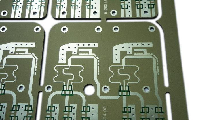
. The land pattern shows the actual land or via shape of the soldered device on the circuit board. These copper patterns on the circuit board also contain some basic shape information. The size of the land pattern needs to be correct to ensure correct soldering and the correct mechanical and thermal integrity of the connected components. When designing the circuit board layout, you need to consider how the circuit board will be manufactured, or how the pads will be soldered if it is soldered manually. Reflow soldering (the flux is melted in a controlled high temperature furnace) can handle a wide range of surface mount devices (SMD). Wave soldering is generally used to solder the reverse side of the circuit board to fix through-hole devices, but it can also handle some surface mount components placed on the back of the circuit board. Generally, when using this technology, the bottom surface mount devices must be arranged in a specific direction, and in order to adapt to this soldering method, the pads may need to be modified.
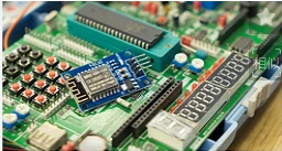
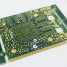
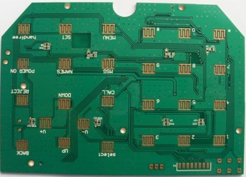
. The selection of components can be changed during the entire design process. Determining which devices should use plated through holes (PTH) and which should use surface mount technology (SMT) early in the design process will help the overall planning of the circuit board. Factors that need to be considered include device cost, availability, device area density, power consumption, and so on. From a manufacturing perspective, surface-mount devices are generally cheaper than through-hole devices and generally have higher availability. For small and medium-scale prototype projects, it is best to choose larger surface mount devices or through-hole devices, which not only facilitate manual soldering, but also facilitate better connection of pads and signals during error checking and debugging.
. If there is no ready-made package in the database, it is usually to create a customized package in the tool.
2. Use a good grounding method
Ensure that the design has sufficient bypass capacitors and ground planes. When using an integrated circuit, make sure to use a suitable decoupling capacitor near the power terminal to the ground (preferably a ground plane). The appropriate capacity of the capacitor depends on the specific application, capacitor technology and operating frequency. When the bypass capacitor is placed between the power and ground pins and placed close to the correct IC pin, the electromagnetic compatibility and susceptibility of the circuit can be optimized.
3. Allocate virtual component packages
Print a bill of materials (BOM) for checking virtual components. Virtual components have no associated packaging and will not be transferred to the layout stage. Create a bill of materials and then view all the virtual components in the design. The only items should be power and ground signals, because they are considered virtual components, which are only processed in the schematic environment and will not be transmitted to the layout design. Unless used for simulation purposes, the components displayed in the virtual part should be replaced with encapsulated components.
4. Make sure you have complete bill of materials data
Check whether there is sufficient data in the bill of materials report. After creating the bill of materials report, it is necessary to carefully check and complete the incomplete device, supplier or manufacturer information in all component entries.
5. Sort according to component label
To facilitate the sorting and viewing of the bill of materials, make sure that the component numbers are consecutively numbered.
6. Check for redundant gate circuits
Generally speaking, the inputs of all redundant gates should have signal connections to avoid dangling the input terminals. Make sure you have checked all redundant or missing gate circuits, and all unwired input terminals are fully connected. In some cases, if the input terminal is suspended, the entire system cannot work correctly. Take the dual op amp that is often used in the design. If only one of the op amps is used in the dual op amp IC components, it is recommended to either use the other op amp, or ground the input of the unused op amp, and deploy an appropriate unity gain (or other gain) ) Feedback network to ensure that the entire component can work normally.
In some cases, ICs with floating pins may not work properly within the specification range. Usually only when the IC device or other gates in the same device are not working in a saturated state-the input or output is close to or in the power rail of the component, this IC can meet the index requirements when it works. Simulation usually cannot capture this situation, because the simulation model generally does not connect multiple parts of the IC together to model the floating connection effect