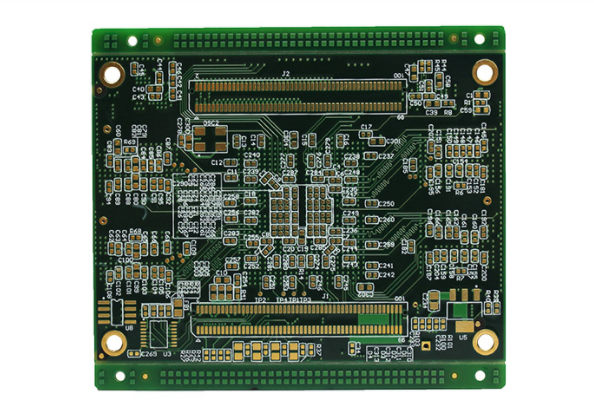
How much distance must be left between the part and the edge of the board during PCB design?
PCB printed circuit board (Printed circuit board, PCB) will appear in almost every kind of electronic equipment. If there are electronic parts in a certain device, they are all mounted on PCBs of different sizes. In addition to fixing various small parts, the main function of the PCB is to provide electrical connections between the upper parts. As electronic devices become more and more complex, more and more parts are needed, and the circuits and parts on the PCB are becoming more and more dense. The base plate of the board itself is made of materials that are insulated and heat-insulated, and not easy to bend.
When designing the PCB, how much distance must be left between the part and the edge of the board so as not to affect the electrical properties? (If the material is FR4, there are SMT parts on both sides, there is a connecting plate design, and there are routing and V-CUT treatments between the plates and the plates) If the width of the Annular ring is increased, can the Tolerance of the finished aperture be more effectively controlled?

This problem has a lot to do with SMT processing equipment. For most equipment, at least 0.150 inch of the board edge is required as a safe distance for assembling the conveying splint. If the panel design is adopted, the fracture processing between the pieces can be V-cut or stamp hole design. It is only necessary to note that the V-cut path retains a width of 20 to 30 mils, and there should not be any residual conductors on it (calculated from the V-ciit center line to both sides), which is ideal. However, some manufacturers deliberately design a line on the V-cut path in order to prevent foolishness, which can be used as an indicator of whether there is a missing cut during electrical testing.
Increasing the width of the Annular ring can indeed effectively control the tolerance of the finished product's aperture. The concept is correct, we can understand from the following points:
(1) In the high current area or independent hole of the PCBA board electroplating process, if the Pad can be enlarged, the average current density can be reduced, and the difference between the hole copper thickness in this area and other areas can naturally be reduced.
(2) The Annular ring is larger, which can also reduce the Solder residue in the hole during the tin spraying process. If other electroplated metal surface treatments are used, the current density can be uniformized and the pore diameter difference can be reduced like copper plating.
iPCB is a high-tech manufacturing enterprise focusing on the development and production of high-precision PCBs. iPCB is happy to be your business partner. Our business goal is to become the most professional prototyping PCB manufacturer in the world. Mainly focus on microwave high frequency PCB, high frequency mixed pressure, ultra-high multi-layer IC testing, from 1+ to 6+ HDI, Anylayer HDI, IC Substrate, IC test board, rigid flexible PCB, ordinary multi-layer FR4 PCB, etc. Products are widely used in industry 4.0, communications, industrial control, digital, power, computers, automobiles, medical, aerospace, instrumentation, Internet of Things and other fields.