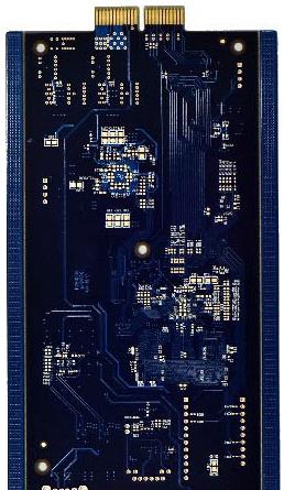
For the little white of PCB design, PCB copper coating is a very difficult technique. Today, the engineer Lao Chen will come to share with you the so-called PCB copper coating techniques and methods. The copper coating of the PCB is to use the idle space on the circuit board as the reference surface, and then fill it with solid copper, so that filling the solid copper is copper filling. The role of copper coating includes
:Reduce the ground wire impedance, improve the anti-interference ability and improve the power efficiency at the same time; connect with the ground wire to reduce the loop area.
The techniques for designing PCB copper coating include:
1. If there are many grounding parts of the PCB, such as SGND, GND, AGND, etc., it is necessary to use the most important "ground" as the standard reference to independently pour copper according to the position of the PCB board and the wiring. The most basic is The digital ground and analog ground are separated for copper plating. Before copper coating, the first thing that should be done is to thicken the corresponding power connection to form multiple deformed structures with different shapes to improve the performance of copper coating.

2. Copper-clad near the crystal oscillator, the crystal oscillator in the circuit is a high-frequency emission source, usually copper is deposited around the crystal oscillator, and then the shell of the crystal oscillator is grounded separately.
3. The single-point connection of different "grounds" is generally connected through a 0 ohm resistor/magnetic bead/inductance;
4. The island (dead zone) problem, if you think it is too big, simply add and define a "ground" via. 5. At the beginning of the wiring, the ground wire should be treated the same. When routing the ground wire, the ground wire should be routed well. You cannot rely on adding via holes to eliminate the ground pins for the connection after copper plating. This effect is very bad.
6. It is best not to have sharp corners on the board (<=180 degrees), because from the perspective of electromagnetics, this constitutes a transmitting antenna! For other things, it is only big or small. I recommend using the edge of the arc.
7. Do not apply copper in the open area of the middle layer of the multilayer board. Because it is difficult for you to make this copper "good grounding"
8. The metal inside the equipment, such as metal radiators, metal reinforcement strips, etc., must be "good grounding".
9. The heat dissipation metal block of the three-terminal regulator must be well grounded. The ground isolation strip near the crystal oscillator must be well grounded. In short: if the grounding problem of the copper on the PCB is dealt with, it is definitely "pros outweigh the disadvantages", it can reduce the return area of the signal line and reduce the electromagnetic interference of the signal to the outside.
Regarding the setting of the copper pour, the safety clearance of the copper pour is generally twice the safety clearance of the wiring. But before there is no copper pour, the safety distance of the wiring is set for the wiring, then in the subsequent copper pour process, the safety distance of the copper pour will also default to the safety distance of the wiring. This is not the same as the expected result.
One stupid way is to double the safety distance after laying out the wires, then pour copper, and then change the safety distance back to the safe distance of the wiring after the copper pour is completed, so that the DRC inspection will not report an error. This method is ok, but if you want to change the copper pour again, you have to repeat the above steps, which is slightly troublesome. The best way is to set a rule for the safety distance of the copper pour separately.
Another way is to add rules. In Rule's Clearance, create a new rule Clearance1 (the name can be customized), and then select Advanced (Query) in the Where the First Object matches option box, click Query Builder, and the Building Query from Board dialog box appears.
In this dialog box, select the default item Show All Levels from the drop-down menu in the first row, select Object Kinds from the drop-down menu under Condition Type/Operator, and select Ploy from the drop-down menu under Condition Value on the right, so that the Query Preview is Is Polygon will be displayed, click OK to confirm, the next step is not finished, and an error will be prompted when it is completely saved:
Next, just change Is Polygon to In Polygon in the Full Query display box, and finally modify the copper safety gap you need in Constraints. Some people say that the priority of the wiring rules is higher than the priority of the copper pour. If the copper pours, it must also comply with the rules of the safe spacing of the wiring. The exception of the copper pour should be added to the rules of the safe spacing of the wiring.
The specific method is to comment not in Polygon in Full Query. In fact, this is completely unnecessary, because the priority can be changed. There is an option priority in the lower left corner of the main page of the rule setting, which increases the priority of the copper-clad safety spacing rule to be higher than the wiring safety spacing rule, so that they can interact with each other. No interference, over.
With the rapid development of electronic products in the direction of portability, miniaturization, networking and multimedia, higher requirements are put forward for the surface mount technology of electronic components and PCB process standards. Facing the future and challenges, PCB factories should welcome the 5G era with more sophisticated products, bring customers more PCB solutions and innovative products, and develop and progress together with customers!