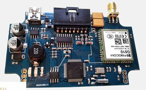
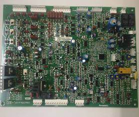
PCB board is the basic electronic component of all electronic circuit design, as the main support, it carries all the components that make up the circuit. The role of PCB is not only to combine scattering components, but also to ensure the regularity of circuit design, and avoid confusion and errors caused by manual cables and wiring.
This article introduces the five key design points of PCB board design in detail.
1. Have a reasonable direction
Such as input and output, AC and DC, strong and weak signals, high frequency and low frequency, high voltage and low voltage. Their directions should be linear (or separated) and should not be intertwined. The purpose is to prevent mutual interference. The best direction is straight, but it is usually difficult to achieve. The most unfavorable trend is the ring. Fortunately, isolation can be improved. For DC, small signal, low voltage PCB board design requirements can be lower. So "reasonable" is relative.

2. Choose a good grounding point: the grounding point is often the most important
Few basic points. I don’t know how many engineers and technicians have discussed it, which shows its importance. Generally speaking, the foundation needs to be shared. For example, multiple ground wires of the preamplifier should be connected, and then connected to the mains. In fact, it is difficult to fully implement due to various restrictions, but you should try to follow it. This question is very flexible in practice. Everyone has their own set of solutions. If it can be explained for a specific circuit board, it can be easily understood.
3. Reasonably arrange power filter decoupling capacitors
Usually, only a few power filter decoupling capacitors are drawn in the schematic diagram, but the location where they should be connected is not pointed out. In fact, these capacitors are used for switching devices (gates) or other components that require filtering and decoupling. These capacitors should be placed as close to these components as possible, if they are too far apart, they will be invalid. Interestingly, when the power supply filter decoupling capacitors are properly placed, the problem of the grounding point is less obvious.
The condition of wide lines should never be fined; high-voltage and high-frequency lines should be smooth, without sharp chamfers, and corners should not be used. The ground wire should be as wide as possible, and it is best to use a large area of copper, which can greatly improve the grounding point problem. The size of the pad or via is too small, or the pad size does not match the hole size. The former is not suitable for manual drilling, and the latter is not suitable for CNC drilling. It is easy to drill the pad into a "c" shape and then drill the pad. The wire is too thin and there is no copper in the large area of the unwired area, which may cause uneven corrosion. That is, when the unwound area is corroded, the thin wire may corrode too much, or it may be damaged or completely broken. Therefore, the role of copper is not only to increase the ground area and anti-interference.
5. Number and line density of via solder joints
In the early stages of circuit production, some problems are not easy to find. They tend to appear later. For example, if there are too many holes, the copper sinking process will cause hidden dangers. Therefore, the design should minimize the number of holes. The straight lines in the same direction are too dense, and it is easy to form a piece when welding. Therefore, the linear density should be determined by the level of the welding process. The distance between the solder joints is too small, which is not conducive to manual soldering, and the welding quality problem can only be solved by reducing the work efficiency. Otherwise it will leave hidden dangers. Therefore, to determine the minimum distance of solder joints, the quality and work efficiency of the soldering personnel should be considered.
If you can fully understand and master the above-mentioned PCB board design precautions, the PCB factory can greatly improve the design efficiency and product quality. Correcting existing errors in the PCB production process will save a lot of time and cost, and save rework time and material investment.