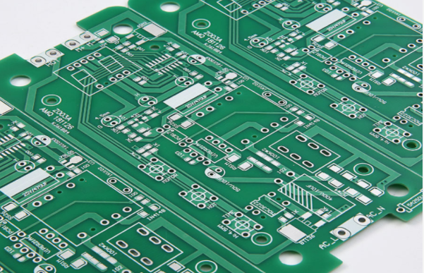
The general principles of multi-layer PCB circuit board layout and wiring PCB designers need to follow the general principles in the circuit board wiring process as follows:
(1) The principle of setting the spacing of printed traces of components. The spacing constraint between different networks is based on the principle of setting the spacing of the printed traces of the components by electrical insulation, manufacturing process, and components. Determined by factors such as size. For example, if the pin pitch of a chip component is 8mil, the [ClearanceConstraint] of the chip cannot be set to 10mil. PCB designers need to set a 6mil PCB design rule for the chip separately. At the same time, the spacing setting should also consider the production capacity of the manufacturer.
In addition, an important factor affecting components is electrical insulation. If the potential difference between two components or networks is large, electrical insulation needs to be considered. The gap safety voltage in a general environment is 200V/mm, which is 5.08V/mil. Therefore, when there are both high-voltage and low-voltage circuits on the same circuit board, it is necessary to pay special attention to sufficient safety clearance. When there are high-voltage circuits and low-voltage circuits, it is necessary to pay special attention to sufficient safety distance.

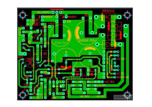
(2) The choice of the wiring form at the corner of the line. In order to make the circuit board easy to manufacture and beautiful, it is necessary to set the corner mode of the circuit and the selection of the wiring form of the corner of the circuit when designing the PCB. Can choose 45°, 90° and arc. Generally, sharp corners are not used. It is best to use arc transition or 45° transition, and avoid 90° or sharper corner transitions.
The connection between the wire and the pad should also be as smooth as possible to avoid small sharp feet, which can be solved by teardropping. When the center distance between the pads is less than the outer diameter D of a pad, the width of the wire can be the same as the diameter of the pad; if the center distance between the pads is greater than D, the width of the wire should not be greater than that of the pad diameter. When a wire passes between two pads without connecting with them, it should keep the largest and equal distance from them. Similarly, when a wire and a wire of a wire pass between two pads without connecting with them, it should be kept to the maximum And equal spacing, the spacing between them should also be uniform and equal and keep the maximum. The spacing between them should also be uniform and equal and kept to the maximum.
(3) How to determine the width of printed traces. The width of the trace is determined by factors such as the level of current flowing through the wire and anti-interference. The larger the overcurrent flowing through the current, the wider the trace should be. The power line should be wider than the signal line. In order to ensure the stability of the ground potential (the larger the change of the ground current, the wider the trace should be. Generally, the power line should be wider than the signal line, and the power line should have less impact than the signal line width), the ground line should also be longer. The wide ground wire should also be wider. Experiments show that when the copper film thickness of the printed wire is 0.05mm, the current carrying capacity of the printed wire should also be wider. It can be calculated according to 20A/mm2, that is, 0.05mm thick, 1mm wide wire can flow through 1A Current. So for the general, the general width can meet the requirements; for high voltage and high voltage, the width of 10~30mil for signal lines can meet the requirements of high voltage and high current signal lines. The line width is greater than or equal to 40mil, line~ The spacing between lines is greater than 30mil. In order to ensure the anti-stripping strength and working reliability of the wire, the widest possible wire should be used to reduce the line impedance and improve the anti-interference performance within the allowable range of the board area and density.
For the width of the power line and ground line, in order to ensure the stability of the waveform, if the wiring space of the circuit board allows, try to thicken it as much as possible. Generally, it needs at least 50mil.
(4) Anti-interference and electromagnetic shielding of printed wires. The interference on the wires mainly includes the interference introduced between the wires, the interference introduced by the power line) the anti-interference and electromagnetic shielding of the printed wires. The interference on the wires mainly includes the interference introduced between the wires, the crosstalk between the signal wires, and the crosstalk between the signal wires, etc. Reasonable arrangement and layout of the wiring and grounding methods can effectively reduce the interference source and make the PCB design The circuit board has better electromagnetic compatibility performance.
For high-frequency or other important signal lines, such as clock signal lines, on the one hand, the traces should be as wide as possible; for high-frequency or other important signal lines, such as clock signal lines, on the one hand, the traces should be as wide as possible. On the other hand, it can be adopted (that is, to wrap the signal line with a closed ground wire, and the package is equivalent to adding a package of ground to isolate it from the surrounding signal lines, which is to use a closed ground wire to separate the signal line." Wrap it up, ground the shield layer). Layer grounding shield layer).