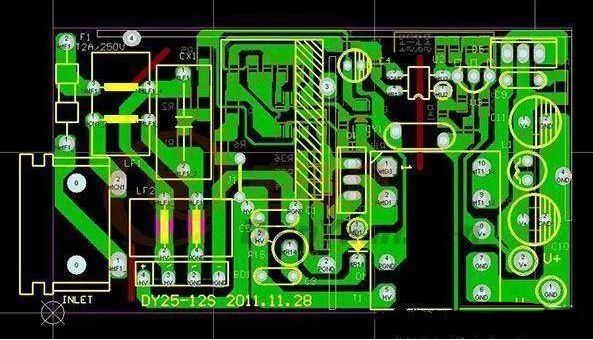
I usually encounter ten classic problems in PCB design, I hope everyone can help you
1. For a group of buses (address, data, command) driving multiple (up to 4, 5) devices (FLASH, SDRAM, other peripherals...), use that method when PCB design and wiring ?
The impact of PCB wiring topology on signal integrity is mainly reflected in the inconsistent signal arrival time at each node, and the reflected signal also arrives at a certain node at inconsistent time, which causes the signal quality to deteriorate. Generally speaking, in a star topology, you can control several stubs of the same length to make the signal transmission and reflection delays consistent to achieve better signal quality.
Before using the topology, it is necessary to consider the situation of the signal topology node, the actual working principle and the wiring difficulty. Different buffers have inconsistent effects on the reflection of the signal, so the star topology cannot solve the delay of the data address bus connected to the flash and sdram, and thus cannot ensure the quality of the signal;
2. In the EMC test, it was found that the harmonics of the clock signal exceeded the standard very seriously, but the decoupling capacitor was connected to the power supply pin. What aspects should be paid attention to in PCB design to suppress electromagnetic radiation?

The three elements of EMC are radiation source, transmission route and victim. The propagation path is divided into space radiation propagation and cable conduction. So to suppress harmonics, first look at the way it spreads. Power supply decoupling is to solve the propagation of conduction mode. In addition, necessary matching and shielding are also required.
3. Is there any regulation on the copper area of the conduction band, that is, the ground plane of the microstrip line?
For microwave circuit design, the area of the ground plane has an impact on the parameters of the transmission line. The specific algorithm is more complicated (please refer to the relevant information of EESOFT by Angelen). In general PCB digital circuit transmission line simulation calculations, the ground plane area has no effect on the transmission line parameters, or ignores the impact.
4. In PCB design, the ground wire is usually divided into protective ground and signal ground; power ground is divided into digital ground and analog ground. Why is the ground wire divided?
The purpose of dividing the ground is mainly for EMC considerations, and it is worried that the noise on the digital part of the power supply and the ground will interfere with other signals, especially analog signals through the conduction path. As for the division of signal and protective ground, it is because the consideration of ESD static discharge in EMC is similar to the role of lightning rod grounding in our lives. No matter how you divide it, there is only one land in the end. It's just that the noise emission method is different.
5. For PCB with frequency above 30M, use automatic wiring or manual wiring when wiring; are the software functions of wiring the same?
Whether the high-speed signal is based on the rising edge of the signal rather than the absolute frequency or speed. Automatic or manual wiring depends on the support of the software wiring function. Some wiring may be better than automatic wiring manually, but for some wiring, such as checking distribution lines, bus delay compensation wiring, the effect and efficiency of automatic wiring will be much higher than manual wiring. Generally, the PCB substrate is mainly composed of a mixture of resin and glass cloth. Due to the different proportions, the dielectric constant and thickness are different. Generally, the higher the resin content, the smaller the dielectric constant, the thinner it can be. For specific parameters, please consult the PCB manufacturer. In addition, with the emergence of new processes, there are also PCB boards of some special materials that are provided for such as ultra-thick backplanes or low-loss RF boards.
6. How to indicate the jumper when the PCB single-layer board is manually wired?
Jumper wire is a special device in PCB design. There are only two pads, and the distance can be fixed-length or variable-length. It can be added as needed during manual wiring. There will be a direct connection on the board, and it will also appear in the bill of materials.
7. Among the products with 4-layer board design, why some are double-sided paving, and some are not?
There are several considerations for the role of paving:
1. Shielding; 2. Heat dissipation; 3. Reinforcement; 4. PCB processing requirements.
So no matter how many layers of slabs are laid, we must first look at the main reasons. Here we mainly discuss high-speed issues, so we mainly talk about shielding. Surface paving is good for EMC, but copper paving should be as complete as possible to avoid islands. Generally, if there are many surface-layer device wiring, it is difficult to ensure the integrity of the copper foil, and it will also bring about the problem of internal signal cross-segmentation. Therefore, it is recommended not to lay copper on the surface-layer devices or boards with many traces.
8. What are the corresponding countermeasures when deploying clock lines of different frequencies?
For the wiring of the clock line, it is best to perform signal integrity analysis, formulate corresponding wiring rules, and perform wiring according to these rules.
9. When the PCB single-layer board is manually wired, should it be placed on the top layer or the bottom layer?
If the device is placed on the top layer, the bottom layer is routed.
10. Is it necessary to add ground wire shields on both sides when fabricating the clock?
Whether to add a shielded ground wire or not depends on the crosstalk/EMI situation on the board, and if the shielded ground wire is not handled well, it may make the situation worse.