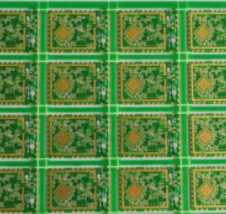
We often find that some mistakes often appear in some rules or facts that we take for granted. Electronic engineers will also have such examples in PCB design.
The following are eight misunderstandings summarized by PCB design engineers.
One: The PCB design requirements of this board are not high, and it is equipped with finer lines and automatic cloth strips. Comments: Automatic wiring will inevitably take up a larger PCB area and produce more holes than manual wiring. In a large number of products, PCB board manufacturers reduce the price. In addition to business factors, the line width and the number of holes will affect the PCB respectively. Output and bit consumption save suppliers' costs, and it has also found a reason to lower prices.

Two: These bus signals are pulled by resistance, don't worry. Comment: There are many reasons why signals need to be pulled up and down, but not all signals need to be pulled. The pull-up resistor pulls a simple input signal, and the current is also tens of microamperes, but when a driving signal is pulled, the current will reach Ma class. Now the system is often 32-bit address data, which may be isolated by 244/245 The bus and other signals are pulled up, and these resistors consume a few watts of power.
Three: How do CPUs and FPGAs do not use I/O ports? Empty it first, and talk about it later. Note: If the I/O port is not used during the pause, a little external interference may become the repeated oscillation of the input signal, and the power consumption of the MOS device basically depends on the number of flips of the gate circuit. If you pull it up, each pin will also have a micro-level current, so the best way is to set the output (of course, no other drive signals can be received outside)
Four: This FPGA has many gates that can be used, and it can be used to the fullest. Note: The power consumption of FGPA is proportional to the number of flip-flops used and the number of flips. Therefore, the power consumption of the same type of FPGA may vary by 100 times at different times in different circuits. Minimizing the number of high-speed flip-flops is the basic method to reduce FPGA power consumption.
Five: The power consumption of these small chips is very low, do not consider. Comment: It is difficult to determine the power consumption of the internal chip that is not too complicated. It mainly depends on the current on the pin. ABT16244, the power consumption without load is less than 1 MA, but its indicator is that each pin can drive 60 loads (for example, matching dozens of Ohm resistance), that is, the full load power consumption is as high as 60 *Of course, 16 = 960mA, only the power supply current is too large, so that the heat falls on the load.
Six: The memory has so many control signals, I only need to use OE and we send out the signal on this board, select the chip on the ground bar, so that the read operation when the data is output is much faster. Note: When the chip selection is valid (regardless of OE and us), most of the memory power consumption is more than 100 times greater than when the chip selection is invalid, so you should use CS to control the chip as much as possible and minimize the chip selection if other requirements are met The width of the pulse.
Seven: Why are these signals rushing? As long as the match is good, it can be eliminated. Note: Except for a few specific signals (such as 100BASE-T, CML), there is overshoot, as long as it is not very large and does not necessarily need to be matched, even if the match does not match the best. For example, the TTL output impedance is less than 50 ohms, and some even 20 ohms. If it is equipped with such a large matching resistance, the current is very large and the power consumption is unacceptable. It cannot be used except for the signal amplitude is too small. The general signal in the output The output impedance of high and low output power is usually different, and there is no way to match it perfectly. Therefore, TTL, LVDS, 422 and other matched signals can be accepted as long as the overshoot.
Eight: It is a matter of hardware personnel that should reduce power consumption as much as possible in the process of PCB factory production, and has nothing to do with software. Comment: The hardware is only a stage. Singing is the software. The bus is accessed by almost every chip, and the flip of each signal is almost completely controlled by the software. If the software can reduce the number of external memory accesses (more use of register variables), and more use of internal CACHE, etc.), timely response to interrupts (interrupts are usually low-level active and with pull-up resistors) and other specific measures for specific boards will make a significant contribution to reducing power consumption.