PCB circuit board design considerations 1
Seven issues that need to be considered in PCB circuit board design! For ease of expression, analysis from the seven aspects of cutting, drilling, wiring, solder mask, characters, surface treatment and forming:
1. Cutting materials mainly consider the issue of plate thickness and copper thickness:
The standard series is 1.0 1.2 1.6 2.0 3.2 MM for the thickness of the sheet material greater than 0.8MM. The thickness of the sheet material is less than 0.8MM and does not count as the standard series. The thickness can be determined according to the needs, but the commonly used thicknesses are: 0.1 0.15 0.2 0.3 0.4 0.6MM, this material is mainly used for the inner layer of multilayer boards.
When designing the outer layer, pay attention to the thickness of the plate. The production and processing need to increase the thickness of copper plating, solder mask thickness, surface treatment (tin spraying, gold plating, etc.) thickness, characters, carbon oil and other thickness. The actual production of sheet metal will be thicker than 0.05-0.1MM, The tin plate will be thicker than 0.075-0.15mm. For example, when the finished product requires a thickness of 2.0 mm during the design, when the 2.0mm sheet is normally selected for cutting, the thickness of the finished sheet will reach 2.1-2.3mm, taking into account the sheet tolerance and processing tolerances. In the meantime, if the design requires that the thickness of the finished plate should not be greater than 2.0mm, the plate should be made of 1.9mm unconventional plate material. The PCB processing plant needs to temporarily order from the plate manufacturer, and the delivery cycle will become very long.

When the inner layer is made, the thickness after lamination can be adjusted by the thickness and structure configuration of the prepreg (PP). The selection range of the core board can be flexible. For example, the thickness of the finished board is required to be 1.6mm, and the choice of the board (core board) can be 1.2 MM can also be 1.0MM, as long as the thickness of the laminated plate is controlled within a certain range, the thickness of the finished plate can be met.
Another issue is the board thickness tolerance. PCB designers should consider the board thickness tolerance after PCB processing while considering the product assembly tolerance. There are three main aspects that affect the tolerance of the finished product, including the incoming material tolerance, lamination tolerance and outer layer thickening tolerance. Several conventional sheet tolerances are now provided for reference: (0.8-1.0)±0.1 (1.2-1.6)±0.13 2.0±0.18 3.0±0.23 Laminating tolerances are controlled within ±(0.05-0.1) according to different layers and thicknesses MM. Especially for boards with board edge connectors (such as printed plugs), the thickness and tolerance of the board need to be determined according to the requirements of matching with the connector.
The surface copper thickness problem, because the hole copper needs to be completed by electroless copper plating and copper electroplating, if no special treatment is done, the surface copper thickness will increase with the thickening of the hole copper. According to the IPC-A-600G standard, the minimum copper plating thickness is 20um for level 1, 2 and 25um for level 3. Therefore, if the copper thickness is required to be 1OZ (minimum 30.9um) when the copper thickness is required during circuit board production, the cutting may sometimes Choose HOZ (minimum 15.4um) cutting material according to the line width/line distance, remove the allowable tolerance of 2-3um, the smallest can reach 33.4um, if you choose 1OZ cutting, the minimum thickness of the finished copper will reach 47.9um. Other copper thickness calculations are available And so on.
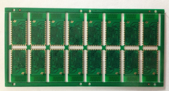
2. Drilling mainly considers the hole size tolerance, the pre-large hole size, the processing problems of the hole to the edge of the board, the non-metalized hole and the design of the positioning hole:
At present, the smallest machining drill bit for mechanical drilling is 0.2mm, but due to the copper thickness of the hole wall and the thickness of the protective layer, the design aperture needs to be enlarged during production, and the spray tin plate needs to be increased by 0.15mm. The gold plate needs to be increased by 0.1mm. The key question here is, if the diameter of the hole is enlarged, will the distance between the hole and the circuit and the copper skin meet the processing requirements? Is the solder ring of the originally designed circuit pad enough? For example, the diameter of the via hole is 0.2mm, The diameter of the pad is 0.35mm. The theoretical calculation shows that 0.075mm on one side of the welding ring can be processed completely, but after the drill is enlarged according to the tin plate, there is no welding ring. If the pads cannot be enlarged by the CAM engineers due to the spacing issue, the board cannot be processed and produced.
Aperture tolerance problem: At present, most of the drilling tolerances of domestic drilling rigs are controlled at ±0.05mm, plus the tolerance of the plating thickness in the hole, the tolerance of metalized holes is controlled at ±0.075mm, and the tolerance of non-metalized holes is controlled at ±0.05mm.
Another problem that is easy to ignore is the isolation distance between the drill hole and the inner copper layer of the multilayer board. Since the hole positioning tolerance is ±0.075mm, there is a tolerance change of ±0.1mm for the expansion and contraction of the inner laminate during lamination. . Therefore, in the design, the distance from the edge of the hole to the line or the copper skin is guaranteed to be above 0.15mm for the 4-layer board, and the isolation of the 6-layer or 8-layer board is guaranteed to be above 0.2mm to facilitate production.
There are three common ways to make non-metallized holes, dry film sealing or rubber particle plugging, so that the copper plated in the hole is not protected by corrosion resistance, and the copper layer on the hole wall can be removed during etching. Pay attention to the dry film sealing, the hole diameter should not be greater than 6.0mm, and the rubber plug hole should not be less than 11.5mm. In addition, secondary drilling is used to make non-metallized holes. No matter what method is adopted, the non-metallized hole must be free of copper in the range of 0.2mm.
The design of positioning holes is often a problem that is easy to overlook. During circuit board processing, testing, shape punching or electric milling, holes larger than 1.5mm are required as positioning holes for board fixation. When designing, it is necessary to consider as much as possible to distribute the holes on the three corners of the circuit board in a triangle shape.