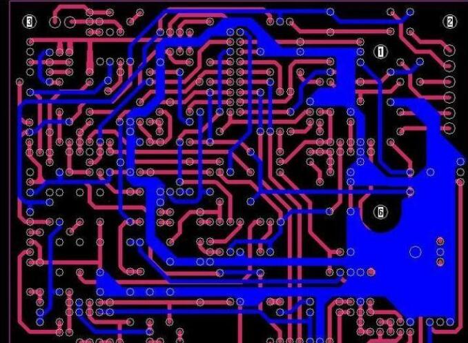
PCB design is very important to power supply circuit design, and it is also one of the technologies that novices must capture. In this article, I will share some of the essences of PCB design.
PCB structure design
In this step, the surface of the PCB board is drawn in the PCB design environment, and the required plug-ins, buttons/switches, screw holes, assembly holes, etc. are placed according to the established board size and various mechanical positions. And consider and determine the wiring area and non-wiring area (for example, various non-wiring areas around screw holes).
1: According to the electrical performance of the reasonable partition, it is generally divided into digital circuit area (fear of interference, interference), analog circuit area (fear of interference), power drive area (interference source);
2: In order to complete the same function of the circuit, place it as close as possible and adjust the components to ensure the simplest connection;
3: For high-quality components, the installation location and installation strength should be considered, heating components should be placed separately from temperature-sensitive components, and heat convection measures should be considered when necessary;
4: The I/O drive components are as close to the edge of the printing plate as possible and close to the lead-out plug-in;
5: The clock generator (such as crystal or clock vibration) should be as close as possible to the device using the clock;
6: Between the power input pin of each integrated circuit and the ground, there is a decoupling capacitor (usually the high-frequency performance of the monoski capacitor);
7: The relay coil should be added to the discharge diode (1N4148 tank);
8: The layout must be balanced, dense, and orderly, not heavy or heavy or heavy.

It is important to note that when placing components, the actual size (occupied area and height) of the components and the relative position between the components must be considered to ensure that the electrical performance of the circuit board and the feasibility of PCB production and installation are both convenient and convenient. At the same time, it should be ensured that the placement of the equipment should be appropriately modified under the premise of reflecting the above principles to make it neat and beautiful. For example, the same equipment should be placed neatly and in the same direction.
This step is related to the overall image of the circuit board and the difficulty of the next wiring, so some work needs to be considered. In the layout, you can first consider the uncertain location, and then fully consider it.
Wiring is the most important operation in the entire PCB design. This will directly affect the performance of the PCB board. In the PCB design process, wiring generally has the following three areas of division: First, layout, which is the most basic requirement for PCB design. If the line is not cloth so that there are flying lines everywhere, it will be an unqualified board and it can be said that it has not been activated.
The second is the satisfaction of electrical performance. This is a measure of whether the printed circuit board is qualified. This is to carefully adjust the wiring after wiping the cloth so that it can achieve the best electrical performance.
Then there is beauty. If the PCB cloth passes through, it will not have any impact on the electrical performance, but it is messy at a glance, plus the colorful and green colors, then even if your electrical performance is good, it will still be garbage debris in the eyes of others. This will bring great inconvenience to testing and maintenance. The wiring should be even, without discipline crossing. These are to ensure electrical performance and meet other individual requirements under implementation, otherwise, this is the end of iPCB.