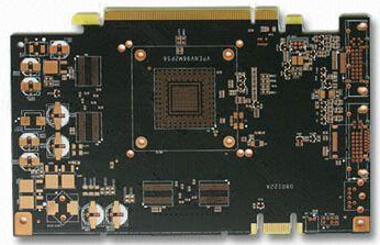
PCB has many layers. When beginners learn PCB design, they are easily confused by various layers. To this end, we put the various layers into the PCB for summary to help you better understand and master.
Definition of the middle layer in PCB design
1: Mechanical Layers
The mechanical layer is usually used to place indicative information about the board and assembly method, such as PCB size, size markings, data, perforation information, assembly instructions and other information.
2: occlusion layer
Used to define the area where components and wiring can be effectively placed on the board. Draw a closed area on this layer as the effective area for wiring, which cannot be automatically arranged and routed.

3: Silk screen layer
The silk screen layer is the text layer, which belongs to the top layer of the PCB and is usually used for annotations.
The top layer (overlay top layer) is used to mark the projection outline of the component, the label of the component, the nominal value or model, and various annotation characters.
The bottom cover is the same as the top silk screen. If all labels are included in the top layer, the bottom silk screen can be turned off.
4: Welding layer (solder resist)
The solder entry layer is the green part of the printed circuit board. In fact, the solder layer uses negative output, so after the shape of the solder layer is mapped to the board, it is not on the unsintered oil-resistant solder but on the copper skin.
5: Multi-layer (multi-layer)
The circuit board pads and penetrating vias penetrate the entire circuit board and establish electrical connections with different conductive pattern layers. Therefore, the system has established an abstraction layer-multi-layer. Usually, the pads and perforations are set to multiple layers. If the layer is turned off, the pads and perforations cannot be displayed.
6: Drill Layer
The drilling layer provides drilling information during the circuit board manufacturing process (for example, a backing board, where through holes need to be drilled).
7: Signal layer
The top signal layer (Top Layer), also known as the component layer, is mainly used to place components. It can be used for double-layer boards and multilayer boards to arrange wires or copper. Bottom signal layer (bottom layer)
Also called soldering layer, it is mainly used for wiring and soldering. It can be used for double-layer boards and multi-layer boards to place components. The intermediate signal layer (middle layer) can use up to 30 layers on the multilayer board in addition to power lines and ground wires. Lay out the signal wires.
8: Internal power layer (internal plane)
Usually referred to as the internal electrical layer for short, it only appears on a multilayer board. The number of PCB layers usually refers to the sum of the signal layer and the internal electrical layer. Like the signal layer, the inner layer and the inner layer, and the inner layer and the signal layer can be connected to each other through through holes, blind holes, and buried holes. Expansion: How many layers is the best PCB design?
According to the number of circuit layers, PCB boards can be divided into single board, double board and multilayer board. So, in PCB design, how many layers are best?
In fact, there is no uniform answer. Instead, PCB designers need to weigh the number of layers to be designed based on the complexity of the entire circuit, mainly from the core equipment of the entire project offline to determine the ease of equipment layout.