As a PCB engineer who has a strong personality and pursuit, how can he draw a complete, efficient and reliable PCB diagram?
The design of PCB proofing seems complicated. It is necessary to consider the direction of various signals as well as energy transmission. The distress caused by interference and heat is also always in the shadows. As long as the PCB design specifications are summarized and summarized, it will be very clear. To put it bluntly, it is a matter of "how to display" and "how to connect".
What to do
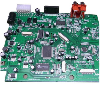
1. Comply with the layout principle of "big first, then small, difficult first, easy first", that is, the priority layout of important unit circuits and core components. This is the same as eating a buffet: buffets are limited in appetite, first pick the ones you like, and when PCB space is limited, pick the important ones first.
Big first and then small, difficult first and easy

2. The heating elements should generally be evenly distributed to facilitate the heat dissipation of the veneer and the whole machine. Temperature sensitive devices other than temperature detection elements should be kept away from large divergent components.
3. Separate components should be properly debugged and repaired, that is, large components cannot be placed around small components, and there must be enough space around components that need to be debugged. It will often become embarrassing if it is too crowded.
Heating components are evenly distributed
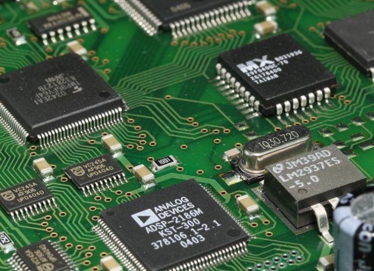
4. The principle diagram should be referred to in the PCB layout, and the main components should be arranged according to the main signal flow law of the single board. The layout should comply with the following requirements: the total connection is shortened and the key signal line is the shortest; the layout of the decapacitor should be as close as possible to the power supply pin of the IC to avoid the shortest loop formed between it and the power supply and ground; reduce the wrong way of signal running, Prevent accidents on the road.
5. For the circuit parts of the same structure, try to use the "symmetrical" standard layout; optimize the layout according to the standard of uniform distribution, balanced center of gravity, and layout appearance.
6. The same type of plug-in components should be placed in one direction in the X or Y direction. The same type of polarized discrete components should also strive to be consistent in the X or Y direction to facilitate production and inspection.
7. High-voltage, high-current signals are completely separated from low-current, low-voltage weak signals; analog signals are separated from digital signals; high-frequency signals are separated from interference signals; the spacing of high-frequency components should be sufficient. The components of the same power supply should be put together as much as possible, and the brakes should be separated from the future power supply.
How to connect
"How to put" is the main consideration for PCB layout, while "how to connect" is relatively more complicated, generally speaking:
1. Rule priority: If there are rules, the signal lines required by the rules will be arranged first, and then the non-critical signal lines will be arranged;
2. Priority of key signal lines: Priority wiring of key signals such as power supply, analog signal, high-speed signal, clock signal, differential signal and synchronization signal;
3. Density priority: Start wiring from the devices with the most complicated single-board connection, and start wiring from the most densely-connected area of the single-board.