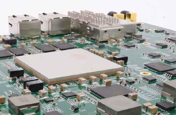
1. Establish component parameters from schematic to PCB design process-input principle netlist-design parameter settings-manual layout-manual wiring-verify design-review-CAM output.
2. Parameter setting The distance between adjacent wires must be able to meet the electrical safety requirements, and in order to facilitate operation and production, the distance should be as wide as possible. The minimum spacing must be at least suitable for the voltage tolerated. When the wiring density is low, the spacing of the signal lines can be increased appropriately. For signal lines with a large gap between high and low levels, the spacing should be as short as possible and the spacing should be increased. Generally, Set the trace spacing to 8mil.
The distance between the edge of the inner hole of the pad and the edge of the PCB board should be greater than 1mm, so as to avoid the defects of the pad during processing. When the traces connected to the pads are thin, the connection between the pads and the traces should be designed into a drop shape. The advantage of this is that the pads are not easy to peel, but the traces and the pads are not easily disconnected.

3, the component layout practice has proved that even if the circuit schematic design is correct and the printed circuit board is not properly designed, it will adversely affect the reliability of electronic equipment. For example, if the two thin parallel lines of the PCB are close together, the signal waveform will be delayed and reflected noise will be formed at the terminal of the transmission line; the interference caused by the improper consideration of the power supply and the ground line will reduce the performance of the product. Therefore, when designing a printed circuit board, attention should be paid to adopting the correct method.
4. Wiring The switching power supply contains high-frequency signals. Any printed line on the PCB can act as an antenna. The length and width of the printed line will affect its impedance and inductance, thereby affecting the frequency response. Even printed lines that pass DC signals can couple to radio frequency signals from adjacent printed lines and cause circuit problems (and even radiate interfering signals again).
5. After the wiring design is completed, it is necessary to carefully check whether the wiring design meets the rules set by the designer, and at the same time, it is necessary to confirm whether the rules made meet the requirements of the PCB production process. Generally check the lines and lines, line and component pads, Whether the distance between the line and the through-hole, the component pad and the through-hole, and the distance between the through-hole and the through-hole is reasonable, and whether it meets the production requirements. Whether the width of the power line and the ground line are appropriate, and whether there is a place to widen the ground line in the PCB. Note: Some errors can be ignored. For example, a part of the outline of some connectors is placed outside the board frame, and errors will occur when checking the spacing; in addition, each time the wiring and vias are modified, the copper must be re-coated.